Aiken Pang and Peter Membrey 2017
Aiken Pang and Peter Membrey Beginning FPGA: Programming Metal 10.1007/978-1-4302-6248-0_1
1. What Is an FPGA and What Can It Do?
F ield- p rogrammable g ate a rrays (FPGA) are a special type of integrated circuits (ICs ) or chip that can be programmed in the field after manufacture and has three basic building blocks: logic gates, flip-flops + memories, and wires. In this chapter we will quickly review what FPGA is and some of the things it can do.
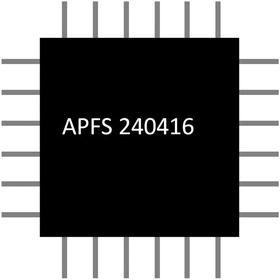
An IC has input and/or output pins (the gray color in Figure ). The black box is the brain of the IC and most ICs have white or gray markings on top of the black box. Most of the ICs mention their specific functions in their datasheet (e.g., is it an amplifier, a processor, a counter, an Ethernet MAC, or a combination of the lot). If you read the FPGA's datasheets and are looking for a specific function, you will probably get very frustrated. Thats because they dont mention the purpose or any of the FPGAs feature sets. All you will be able to find is how many logic gates, how much memory, and how to program the FPGA, but you wont find functions or features. You just cannot figure them out from the datasheet.
Figure 1-1.
Integrated circuits, or chip, look like this
FPGAs allow designers to modify their designs very late in the design cycle even after the end product has been manufactured and deployed in the field. Sound familiar? It should sound a lot like Windows updates or Android/Apple phone software updates. That's one of the most powerful and compelling features of an FPGA but please dont treat FPGA design as a software programming exercise for a microcontroller or processor. An FPGA is not a processor with software. It is an amazing device that allows the average person to create his or her very own digital circuit. You are designing a hardware digital circuit when you are creating an FPGA design. You are going to use a hardware description language (which, incidentally, is used by Intel CPU chip designers too) to design your FPGA. This is a very important concept. We will provide more details when we are putting together some example designs in the later chapters. In the following sections well provide a little bit more detail about field-programmable, gates, and arrays and what they can do.
1.1 Field-Programmable
The most valuable FPGA feature is that the end user can program or configure it within seconds. This means that the end user can change the hardware design in the FPGA chip quickly and at will. For example, the FPGA can change from temperature sensor to LED (light-emitting diode) driver within a few seconds. This means that FPGAs are useful for rapid product development and prototyping. This field-programmable magic is done by a configuration file, often called a bit file which is created by a designer (you). Once loaded, the FPGA will behave like the digital circuit you designed!
1.1.1 Configuration Technology
Table lists the three types of configuration technologies : static random access memory (SRAM) , flash memory , and antifuse.
Table 1-1.
Different Types of Configuration Technology
| SRAM | Flash | Antifuse |
|---|
Achronix | YES | -- | -- |
Altera | YES | -- | -- |
Lattice | YES | -- | -- |
Microsemi | -- | YES | YES |
Xilinx | YES | -- | -- |
Most of the FPGA vendors are using SRAM technology. It is fast and small, and it offers unlimited reprogrammability. One of the drawbacks though is that the FPGA needs time to reload the entire design into SRAM every time you power up the FPGA. This approach also takes more power.
Flash and antifuse technologies are non-volatile (meaning that they can retain data even if the power is turned off) so that they provide the benefit of instant on without needing to reload the FPGA bit file every time we power up the FPGA or the system. They also draw less power than the SRAM approach.
Antifuse technology can only be programmed once and cant match the performance of SRAM technology. The only reasons to use an antifuse technology FPGA today is due to its super high reliability and security.
Tips
The worlds largest and most powerful particle acceleratorLarge Hadron Collider (LHC)uses antifuse FPGAs to implement radiation protection digital circuits.
This book focuses on SRAM technology because it is the most common technology and is the easiest to program. Most of the SRAM-based FPGAs have an external EEPROM (electrically erasable programmable read-only memory) for storing the bit file, similar to how a computer stores programs on disk. All you need to do is burn your bit file into the EERPOM and the FPGA will autoload the bit file from the EEPROM when it powers up.
1.2 Gates = Logic
The gate is the most basic element in digital logic and is more formally known as a logic gate. All modern digital designs are based on CMOS (complementary metal oxide semiconductor) logic gates. To support complex digital designs, FPGAs contain tens of thousands, hundreds of thousands, or even more individual logic elements which are built by logic gates.
1.2.1 The Basic Gate Design Block No. 1: Logic Element
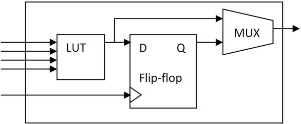
The logic element (LE) is one of the smallest elements in FPGA design. It basically consists of a look-up table (LUT) , flip-flop, and multiplexer (which we will cover shortly). FPGAs are used extensively for compute problems that can benefit from parallel computing architecturesfor example, cleaning up images being received from an image sensor, local processing on image pixels, and computing difference vectors in H.264 compression. LEs can form any complex or even simple digital function inside the FPGA. Figure . Most of the inputs to a LE are connected to the LUT and followed with a flip-flop (register). The output of the LE is selected by a multiplexer (MUX) . The LUT and MUX are the major configurable blocks in the LE. Dont worry, this will all make sense after you read the next section.
Figure 1-2.
Basic configurable LEs
1.2.1.1 The Magic Block: LUT
The LUT is basically just a small amount of read-only memory. A four-input, one output LUT, can generate any four-input Boolean function (AND/OR/XOR/NOT) (Figure ). In some FPGA LE designs, LUTs can be combined to form a 16-bit shift register or memory block. There is another similar block, the MUX, in the basic LE. It is used to select the output source from a register or directly from LUT. In reality, the LEs are a bit more complex in that they may very well have more than one LUT and MUX.

