1.1 Introduction
The FPGA or field-programmable gate array is a wonderful technology used by electronic system developers to design, debug, and implement unique hardware solutions without having to develop custom silicon devices. Xilinx is a semiconductor manufacturer of standard FPGA chips which are sold blank or unprogrammed to customers. The customers then program these devices to implement their unique systems. If a feature changes or a bug is discovered, the user can simply load a new program to the FPGA to create a new product or upgrade. This process can even continue after shipment in the form of firmware upgrades. The act of programming the FPGA is called configuration to distinguish it from loading any associated software programs. With modern FPGAs however, the line is blurring between hardware configuration and software programming.
All this programmability requires additional silicon area compared to hard ASIC (application-specific integrated circuit) implementations of the same logic. This is because in ASIC implementations the gates and wiring are fixed. This area cost penalty can be in the 1.510X range for FPGAs. However, the ASIC also must include the development cost and schedule which can be in the range of $10$500 million dollars and can take several years with teams of hundreds of developers. With each generation of lithography, the cost to develop an ASIC increases. For these reasons, most medium-sized and smaller systems rely on a mix of FPGAs for customization along with standard ASIC or ASSPs and memories.
This revolutionary technology has impacted the electronic product development cycle for nearly all electronic devices since its introduction in the late 1980s.
1.2 The Evolution of Programmable Logic
The initial user programmable devices called PLDs ( programmable logic devices ) that were developed in 1978 by MMI could replace ten or so TTL gates and were one time programmable. This led to the reprogrammable PLDs based on EEPROM or EPROM technologies.
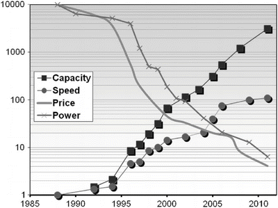
By 1985 advancing lithography enabled a new class of device, the FPGA. FPGAs introduced two important new architecture features: programmable routing to interconnect the increasing number of gates on a device and a programmable gate called a LUT or lookup table with an associated register. The initial devices from Xilinx contained up to a hundred LUT and flip-flop pairs in a basic logic element called a CLB or configurable logic block . Rather than using a permanently programmed EPROM or EEPROM memory, Xilinx FPGAs relied on CMOS memories to hold programming information. Figure illustrates the technological improvement of modern FPGAs relative to the original Xilinx XC2064 which had 64 programmable logic cells.
Fig. 1.1
FPGA evolution since the 1980s
The FPGA took its place as a central component in digital systems, replacing PLDs and TTL for implementing glue logic. In the 1990s new uses began to emerge for FPGAs, which were becoming more capable than just gluing I/O to processors. The emerging Internet became a growth driver for FPGAs with FPGAs being used for prototyping, initial deployment, and full-scale production of Internet switches and routers. By 2000 communications systems were the primary market for FPGAs. Other new markets for FPGAs also emerged for ASIC prototyping (Chap. ) and PicoBlaze architectures.
The original FPGA architecture was a simple implementation of a programmable logic block. With each new generation, new programmable functions have been added along with hardening of some specific functions in order to reduce the cost or improve the performance of FPGAs in digital systems. These blocks continue to evolve in each generation. Many important functions have been added since the initial FPGAs including the following:
Fast carry chains for high-speed adders and counters
Small memories called distributed RAMs (or LUTRAMs)
Block memories (BRAM or block RAMs)
A hard RISC processor block based on the PowerPC
Multi-Gigabit or MGT serial transceivers
The DSP48 for digital signal processing
Hard PCI blocks
A complete system on chip (SoC) as a hard block in the FPGA in the Zynq family of FPGAs
The inclusion of hard blocks in FPGAs is driven by the trade-off between usage and cost. For customers which use these functions, value and performance are increased; however, if these hard blocks are not used, they are wasted space which can increase cost. Additionally these hard functions require significant software support to be useful to customers. For these reasons, hardening functions have been limited to those functions of clear value in important market verticals.
1.4 Application Level System Architectures
The above applications in turn identify the need for the following system level usage, which might be applicable in multiple markets.
1.4.1 Glue Logic and Custom Interface IP
This was the original use case for early FPGAs. Typically the FPGA is used to interface a processor IC to a variety of I/O devices and memory-mapped devices. This use case requires low-cost FPGAs with plentiful I/O. Key features are combinatorial programmable logic nets, IOBs, and internal registers.
Often an application will require a custom interface such as an industrial interface or perhaps multiple interfaces such as USB. If these interfaces are not available in the users SoC, they can be implemented in a companion FPGA.
1.4.2 Communications Switch
Multiple interfaces of various standards and performance levels such as 10G Ethernet are connected together via an FPGA implemented switch. These switches are common in Internet, industrial, and video networks.
1.4.3 I/O Stream Processing
FPGAs are ideal devices to connect to high-bandwidth real-time I/O streams such as video, radio, radar, and ultrasound systems. Often the system is used to reduce the high-native bandwidth of the I/O stream to levels manageable for a processor. For instance, a radio front end may sample A/D data at 1 GHz but after down conversion produces a more moderate rate of 10 MB/s. Conversely lower-bandwidth data may be up converted to a high-bandwidth I/O stream. Another example is a video system with a frame buffer which may be updated infrequently, but the video output stream is a real-time high-bandwidth stream.

