Dasgupta Anindya - Design and control of matrix converters: regulated 3-phase power supply and voltage sag mitigation for linear loads
Here you can read online Dasgupta Anindya - Design and control of matrix converters: regulated 3-phase power supply and voltage sag mitigation for linear loads full text of the book (entire story) in english for free. Download pdf and epub, get meaning, cover and reviews about this ebook. City: Singapore, year: 2017, publisher: Springer, genre: Computer. Description of the work, (preface) as well as reviews are available. Best literature library LitArk.com created for fans of good reading and offers a wide selection of genres:
Romance novel
Science fiction
Adventure
Detective
Science
History
Home and family
Prose
Art
Politics
Computer
Non-fiction
Religion
Business
Children
Humor
Choose a favorite category and find really read worthwhile books. Enjoy immersion in the world of imagination, feel the emotions of the characters or learn something new for yourself, make an fascinating discovery.

- Book:Design and control of matrix converters: regulated 3-phase power supply and voltage sag mitigation for linear loads
- Author:
- Publisher:Springer
- Genre:
- Year:2017
- City:Singapore
- Rating:5 / 5
- Favourites:Add to favourites
- Your mark:
Design and control of matrix converters: regulated 3-phase power supply and voltage sag mitigation for linear loads: summary, description and annotation
We offer to read an annotation, description, summary or preface (depends on what the author of the book "Design and control of matrix converters: regulated 3-phase power supply and voltage sag mitigation for linear loads" wrote himself). If you haven't found the necessary information about the book — write in the comments, we will try to find it.
Dasgupta Anindya: author's other books
Who wrote Design and control of matrix converters: regulated 3-phase power supply and voltage sag mitigation for linear loads? Find out the surname, the name of the author of the book and a list of all author's works by series.


Design and control of matrix converters: regulated 3-phase power supply and voltage sag mitigation for linear loads — read online for free the complete book (whole text) full work
Below is the text of the book, divided by pages. System saving the place of the last page read, allows you to conveniently read the book "Design and control of matrix converters: regulated 3-phase power supply and voltage sag mitigation for linear loads" online for free, without having to search again every time where you left off. Put a bookmark, and you can go to the page where you finished reading at any time.
Font size:
Interval:
Bookmark:
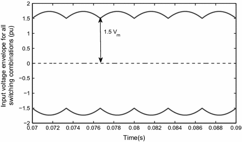
 . This results in a pulsating voltage
  at the output. The DC component of
  can be obtained by averaging the pulse waveform over the switching period
  as
as 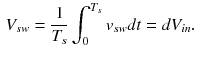
 . The switching frequency (
  ) components and its harmonics which are also present in
  can be subsequently attenuated to a large extent by using a LC filter. The important point to note here is that any desirable value of the DC component of the output voltage can be generated as long as this value is less than the source voltage
  .
. 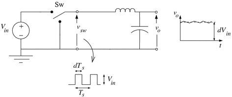

 is 0.866 times that of the input line-line voltage amplitude. Within this amplitude limit, a fundamental component of
  having any amplitude, phase and frequency can be produced by appropriately regulating the SPTT switches.
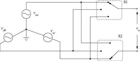

Font size:
Interval:
Bookmark:
Similar books «Design and control of matrix converters: regulated 3-phase power supply and voltage sag mitigation for linear loads»
Look at similar books to Design and control of matrix converters: regulated 3-phase power supply and voltage sag mitigation for linear loads. We have selected literature similar in name and meaning in the hope of providing readers with more options to find new, interesting, not yet read works.
Discussion, reviews of the book Design and control of matrix converters: regulated 3-phase power supply and voltage sag mitigation for linear loads and just readers' own opinions. Leave your comments, write what you think about the work, its meaning or the main characters. Specify what exactly you liked and what you didn't like, and why you think so.