In the last years, the proliferation of consumer electronic devices triggered a huge increase in microelectronic activities, enabling the growth of integrated circuits (ICs) market from $10 billion in 1980 to over than $340 billion in 2015, with the analog market growing 10.6% in 2014, 0.7 points over the overall market growth, and expected to follow in 2015 (World Semiconductor Trade Statistics (WSTS), https://www.wsts.org/ ; McClean, IC Market to Top $300 Billion for First Time in 2013, http://www.icinsights.com ). The steady increase in overall performance of ICs has been mostly supported by an exponential growth in the density of transistors while inversely reducing the transistors cost, as described by Moores law (Proc. IEEE 86:8285, 1998). Due to the developments made in the last decades in very large scale integration technologies, designers have the means to build extremely complex multimillion transistor ICs that implement complete systems in a single chip. The need of new functionalities, smaller devices, more power efficiency, less production and integration costs, and less design cost makes the design of electronic systems a truly challenging task, which must be completed within strict time-to-market constraints. The accomplishment of this complex task is only possible since designers are assisted by computer-aided design (CAD) tools that support the whole design process.
1.1 The AMS IC Design Flow
Even though most functions in todays ICs are implemented using digital or digital signal processing circuitry, analog circuits are the link between digital circuitry and the continuous-valued external world [] is a common practice.
Due to the continuous nature of the signal values handled by analog circuits, they are much more sensitive to noise and process variations than their digital counterpart, leading to a more complex and time demanding design. Hence, designers have been replacing most of analog circuits by digital computations, however, the following list enumerates some typical blocks referred as remaining analog forever []:
On the input side of a system, the signals from a sensor, microphone or antenna must be sensed or received, amplified and filtered up to a level that allows digitalization with satisfying signal-to-noise and distortion ratio. Typical application of these circuits is in sensor interfaces, telecommunication receivers or sound recording;
On the output side of a system, the signal from digital processing must be reconverted to analog and it has to be strengthened, so that it can drive outside load with low distortion. These circuits are typically used in telecommunication transmitters and loudspeakers;
Mixed-signal circuits like sample-and-hold, analog-to-digital converters and frequency synthesizers. These blocks establish the interface between input/output sides of a system and digital processing parts of a SoC;
Voltage or current reference circuits, and also, crystal oscillators, to offer stable and absolute references for the above mentioned circuitry;
The last block of analog circuits are the high-performance digital circuits. The prime example is state-of-the-art microprocessors that are customized like AMS circuits, attempting to reach higher speed and lower power consumption.
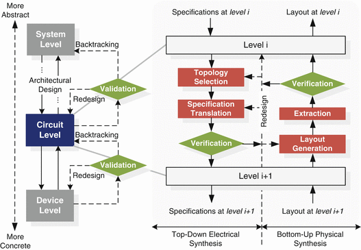
In terms of design flow specific for analog IC, it is acknowledged that each designer or company may have its own IC design flow. However, Gielen and Rutenbar [. It consists of a series of top-down design steps repeated from the system-level to the device-level, and bottom-up layout generation and verification.
Fig. 1.1
Hierarchical levels and design tasks of AMS IC design process []
By adopting a hierarchical top-down design methodology is possible to perform system architectural exploration, obtaining a better overall system optimization at a higher abstraction level before starting more detailed implementations at the circuit- or device-level. Thus, attempting to find problems earlier in the AMS design flow increase the chances of first-time success, with fewer or no overall time consuming redesign iterations []. Nonetheless, the increased impact of layout parasitics and process variations with the state-of-the-art integration technologies is forcing many iterations in real world designs.
In this design flow the number of hierarchy levels depends on the complexity of the system being handled and there are no generally accepted representations for the architectural design, however, the steps between any two hierarchical levels are:
Top-down electrical synthesis path, that includes topology selection, specification translation (or circuit sizing at the lowest level) and design verification;
Bottom-up physical synthesis path, that includes layout generation and detailed design verification (after layout extraction).
Topology selection is the step of determining the most appropriate system or circuit topology in order to meet a set of given specifications at the current hierarchy level. The topology can be either chosen from a set of available topologies, or synthetized.
Specification translation is the task of mapping the high-level block specifications, given a selected topology, into individual specifications for each of the sub-blocks. At the lowest level, the sub blocks are single devices and this task is reduced to circuit sizing. Specifications translation is verified by means of simulation before proceeding down the hierarchy. Since no device-level sizing is available at higher levels, simulations, at these levels, are behavioral. However, at the lowest levels in the design hierarchy, the circuit- and device-level, device sizing is available and, therefore, electrical simulations are used. The specifications for each of the blocks are passed to the next level of the hierarchy and the process is repeated until the top-down electrical synthesis flow is completed.
Several CAD tools, settled through the years in the industry, are fundamental to help the designer to successfully complete the circuit sizing task. They are used for IC design editing and evaluation, some of the tools available are: Mentor Graphics ADiT, Questa and Eldo []. Even if applicable only at cell-level, i.e., generally analog components with 10100 devices, they increase the automation level of the analog design environment.
From the bottom-up physical synthesis path, layout generation consists of creating the fabrication masks that are used to produce the devices. For the blocks at the lowest level in the design hierarchy this involves drawing the set of geometric shapes, which must obey strict design rules defined by the manufacturing process, that implement the intended devices and interconnections. For blocks at higher levels it involves placing and routing the layouts of the previously designed sub-blocks. In the provided design flow, is important to notice the presence of a detailed verification step over the extraction of the layout parasitics. In order to ascend to higher hierarchical levels is necessary that no potential problems are detected at the lowest levels and the circuit meets the target specifications after layout, i.e., post-layout verification. If not, backtracking and redesign steps are required. When the topmost level verification is complete, the system is designed and ready for fabrication.


