R. Jacob Baker - CMOS: Circuit Design, Layout, and Simulation; 3rd Edition (IEEE Press Series on Microelectronic Systems)
Here you can read online R. Jacob Baker - CMOS: Circuit Design, Layout, and Simulation; 3rd Edition (IEEE Press Series on Microelectronic Systems) full text of the book (entire story) in english for free. Download pdf and epub, get meaning, cover and reviews about this ebook. year: 2010, publisher: Wiley-IEEE, genre: Computer. Description of the work, (preface) as well as reviews are available. Best literature library LitArk.com created for fans of good reading and offers a wide selection of genres:
Romance novel
Science fiction
Adventure
Detective
Science
History
Home and family
Prose
Art
Politics
Computer
Non-fiction
Religion
Business
Children
Humor
Choose a favorite category and find really read worthwhile books. Enjoy immersion in the world of imagination, feel the emotions of the characters or learn something new for yourself, make an fascinating discovery.

- Book:CMOS: Circuit Design, Layout, and Simulation; 3rd Edition (IEEE Press Series on Microelectronic Systems)
- Author:
- Publisher:Wiley-IEEE
- Genre:
- Year:2010
- Rating:4 / 5
- Favourites:Add to favourites
- Your mark:
CMOS: Circuit Design, Layout, and Simulation; 3rd Edition (IEEE Press Series on Microelectronic Systems): summary, description and annotation
We offer to read an annotation, description, summary or preface (depends on what the author of the book "CMOS: Circuit Design, Layout, and Simulation; 3rd Edition (IEEE Press Series on Microelectronic Systems)" wrote himself). If you haven't found the necessary information about the book — write in the comments, we will try to find it.
R. Jacob Baker: author's other books
Who wrote CMOS: Circuit Design, Layout, and Simulation; 3rd Edition (IEEE Press Series on Microelectronic Systems)? Find out the surname, the name of the author of the book and a list of all author's works by series.


CMOS: Circuit Design, Layout, and Simulation; 3rd Edition (IEEE Press Series on Microelectronic Systems) — read online for free the complete book (whole text) full work
Below is the text of the book, divided by pages. System saving the place of the last page read, allows you to conveniently read the book "CMOS: Circuit Design, Layout, and Simulation; 3rd Edition (IEEE Press Series on Microelectronic Systems)" online for free, without having to search again every time where you left off. Put a bookmark, and you can go to the page where you finished reading at any time.
Font size:
Interval:
Bookmark:
Contents
Square-Law Equations
For a triode-operating long-channel NMOS device
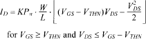
For a long-channel NMOS device operating in the saturation region:
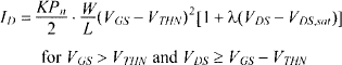
On the border between saturation and triode:
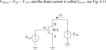
V DS,sat = V GS V THN and the drain current is called I D,sat , see
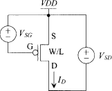
For the PMOS device equations make the following substitutions in the equations listed above
V DS V SD , V GS V SG , and V THN V THP .
All of the voltages and currents in the PMOS and NMOS equations are positive. For example, for the PMOS device to conduct a drain current requires V SG > V THP . For the NMOS to conduct a drain current requires V GS > V THN .
CMOS
IEEE Press
445 Hoes Lane
Piscataway, NJ 08854
IEEE Press Editorial Board
Lajos Hanzo, Editor in Chief
| R. Abari | M. El-Hawary | S. Nahavandi |
| J. Anderson | B. M. Hammerli | W. Reeve |
| F. Canavero | M. Lanzerotti | T. Samad |
| T. G. Croda | O. Malik | G. Zobrist |
Kenneth Moore, Director of IEEE Book and Information Services (BIS)
IEEE Solid-State Circuits Society, Sponsor
Copyright 2010 by the Institute of Electrical and Electronics Engineers, Inc. All rights reserved.
Published by John Wiley & Sons, Inc., Hoboken, New Jersey.
Published simultaneously in Canada.
No part of this publication may be reproduced, stored in a retrieval system, or transmitted in any form or by any means, electronic, mechanical, photocopying, recording, scanning, or otherwise, except as permitted under Section 107 or 108 of the 1976 United States Copyright Act, without either the prior written permission of the Publisher, or authorization through payment of the appropriate per-copy fee to the Copyright Clearance Center, Inc., 222 Rosewood Drive, Danvers, MA 01923, (978) 750-8400, fax (978) 750-4470, or on the web at www.copyright.com . Requests to the Publisher for permission should be addressed to the Permissions Department, John Wiley & Sons, Inc., 111 River Street, Hoboken, NJ 07030, (201) 748-6011, fax (201) 748-6008, or online at http://www.wiley.com/go/permission .
Limit of Liability/Disclaimer of Warranty: While the publisher and author have used their best efforts in preparing this book, they make no representations or warranties with respect to the accuracy or completeness of the contents of this book and specifically disclaim any implied warranties of merchantability or fitness for a particular purpose. No warranty may be created or extended by sales representatives or written sales materials. The advice and strategies contained herein may not be suitable for your situation. You should consult with a professional where appropriate. Neither the publisher nor author shall be liable for any loss of profit or any other commercial damages, including but not limited to special, incidental, consequential, or other damages.
For general information on our other products and services or for technical support, please contact our Customer Care Department within the United States at (800) 762-2974, outside the United States at (317) 572-3993 or fax (317) 572-4002.
Wiley also publishes its books in a variety of electronic formats. Some content that appears in print may not be available in electronic format. For information about Wiley products, visit our web site at www.wiley.com .
Library of Congress Cataloging-in-Publication Data:
Baker, R. Jacob, 1964
CMOS: circuit design, layout, and simulation / Jake Baker. 3rd ed.
p. cm.
Summary: The third edition of CMOS: Circuit Design, Layout, and Simulation continues to cover the practical design of both analog and digital integrated circuits, offering a vital, contemporary view of a wide range of analog/digital circuit blocks, the BSIM model, data converter architectures, and much more. The 3rd edition completes the revised 2nd edition by adding one more chapter (chapter 30) at the end, which describes on implementing the data converter topologies discussed in Chapter 29. This additional, practical information should make the book even more useful as an academic text and companion for the working design engineer. Images, data presented throughout the book were updated, and more practical examples, problems are presented in this new edition to enhance the practicality of the bookProvided by publisher.
Summary: The third edition of CMOS: Circuit Design, Layout, and Simulation continues to cover the practical design of both analog and digital integrated circuits, offering a vital, contemporary view of a wide range of analog/digital circuit blocks, the BSIM model, data converter architectures, and much moreProvided by publisher.
ISBN 978-0-470-88132-3 (hardback)
1. Metal oxide semiconductors, ComplementaryDesign and construction. 2. Integrated circuitsDesign and construction. 3. Metal oxide semiconductor field-effect transistors. I. Title.
TK7871.99.M44B35 2010
621.39732dc22 2010016630
To my wife Julie
Preface
CMOS (complementary metal oxide semiconductor) technology continues to be the dominant technology for fabricating integrated circuits (ICs or chips). This dominance will likely continue for the next 25 years and perhaps even longer. Why? CMOS technology is reliable, manufacturable, low power, low cost, and, perhaps most importantly, scalable. The fact that silicon integrated circuit technology is scalable was observed and described in 1965 by Intel founder Gordon Moore. His observations are now referred to as Moores law and state that the number of devices on a chip will double every 18 to 24 months. While originally not specific to CMOS, Moores law has been fulfilled over the years by scaling down the feature size in CMOS technology. Whereas the gate lengths of early CMOS transistors were in the micrometer range (long-channel devices) the feature sizes of current CMOS devices are in the nanometer range (short-channel devices).
To encompass both the long- and short-channel CMOS technologies in this book, a two-path approach to custom CMOS integrated circuit design is adopted. Design techniques are developed for both and then compared. This comparison gives readers deep insight into the circuit design process. While the square-law equations used to describe MOSFET operation that students learn in an introductory course in microelectronics can be used for analog design in a long-channel CMOS process they are not useful when designing in short-channel, or nanometer, CMOS technology. The behavior of the devices in a nanometer CMOS process is quite complex. Simple equations to describe the devices behavior are not possible. Rather electrical plots are used to estimate biasing points and operating behavior. It is still useful, however, for the student to use mathematical rigor when learning circuit analysis and design and, hence, the reason for the two-path approach. Hand calculations can be performed using a long-channel CMOS technology with the results then used to describe how to design in a nano-CMOS process.
Font size:
Interval:
Bookmark:
Similar books «CMOS: Circuit Design, Layout, and Simulation; 3rd Edition (IEEE Press Series on Microelectronic Systems)»
Look at similar books to CMOS: Circuit Design, Layout, and Simulation; 3rd Edition (IEEE Press Series on Microelectronic Systems). We have selected literature similar in name and meaning in the hope of providing readers with more options to find new, interesting, not yet read works.
Discussion, reviews of the book CMOS: Circuit Design, Layout, and Simulation; 3rd Edition (IEEE Press Series on Microelectronic Systems) and just readers' own opinions. Leave your comments, write what you think about the work, its meaning or the main characters. Specify what exactly you liked and what you didn't like, and why you think so.