1.1 Charge carriers, crystal structure and conductivity
You should be familiar with some very basic concepts of matter and electrical quantities such as charge, current and voltage in order to describe the operation of electronic circuits. Matter consists of atoms made of a nucleus which is orbited by negatively charged electrons. The nucleus itself is made up of positively charged protons and neutrons without an electrical charge. Electric charge is measured in coulombs (C). The smallest fundamental unit of electrical charge is a physical constant called the elementary positive charge:
All charges are an integer multiple of this elementary charge. The proton has a charge of +e while the electron has a charge of e.
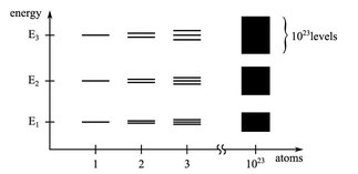
As a consequence of quantum mechanics, the electrons of a single isolated atom (not interacting with other atoms) can occupy only discrete energy levels (atomic orbitals), see .
: Splitting of discrete energy levels into energy bands for increasing number of atoms.
If several atoms form a molecule by chemical bonding the atomic orbitals split into separate molecular orbitals with different energy levels. shows this splitting of energy levels: For an H2 molecule with two atoms the energy levels of the single atoms split into two energy levels with the lower energy level being occupied by two electrons. In general the outermost electrons (valence electrons) can participate in the formation of chemical bonds with other atoms to form molecules, in solid, liquid or gaseous states.
When a large number of atoms form a solid the number of orbitals (proportional to the number of valence electrons) becomes very large and the difference in energy between these orbitals becomes very small. In consequence solids (with about 1023 or more atoms) show continuous energy bands rather than discrete energy levels. The energy bands can overlap or are separated by intervals of energy without orbitals (electrons within the solid cannot have these energies). These forbidden energy intervals are called band gaps and the total of bands and band gaps is called the band structure.
shows a simplified diagram of the electronic band structure of crystalline solids on the right. The shape of the band structure depends on the atoms forming the solid and its crystal structure.
metal (left); semiconductor (center); insulator (right).
The electric properties of a solid are mainly determined by the band structure around the so-called Fermi level (see conduction band. Conductivity occurs if the conduction band is partly filled by electrons or electrons are missing in the valence band.
1.2 The electrical properties of solids
Electrical properties can be distinguished depending on the presence and size of a band gap at the Fermi level.
Metals
The valence and conduction band overlap (the Fermi level lies within this overlapping band) or the Fermi level lies within the conduction band (not shown) and therefore the band is partly filled with electrons regardless of temperature. These electrons form a sea of practically free electrons moving in the background of the positively charged crystal structure ().
: The crystal structure of a metal: positively charged atomic cores surrounded by delocalized free electrons.
Insulators
In an conduction band is empty, resulting in no conductivity. At higher temperatures electrons can be excited to the conduction band due to thermal energy (leaving a hole in the valence band), but at reasonable temperatures the number of excited electrons is negligible and there is no conductivity.
Examples of insulators are glass or plastic materials, see .
Semiconductors
Like for insulators the Fermi level for pure semiconductors, (also known as intrinsic semiconductors), is within a band gap of width E, but this time the band gap is smaller. Semiconductors are isolators at absolute zero. Thanks to the smaller band gap, electrons can be excited to the conduction band more easily due to thermal energy. As the excitation of electrons is a thermal effect the number of intrinsic electrons in the conduction band ni is strongly temperature dependent:
Here kB=1.3810-23 J/K which is the Boltzmann constant.
When an electron is excited to the conduction band this electron is missing in the valence band. This missing electron is called an electron hole, or defect electron and also contributes to conductivity. The density of holes is the same as the density of excited electrons. The conductivity of semiconductors is higher than that of insulators, but still significantly lower than that of metals.
Fig. 1.4: The crystal structure of silicon.
As every excited electron generates a hole the density of electrons n0 and holes p0 is the same and corresponds to the intrinsic charge carrier density ni:
The opposite of the generation of electron-hole pairs is called recombination. The recombination rate depends on the carrier density of electrons and holes. The rate of generation and recombination of electron-hole pairs is temperature dependent. In thermal equilibrium both rates are the same and the number of free electron-hole pairs is constant at the given temperature. The equality of the two rates leads to the mass action law:
The product of the charge density of the free electrons and holes equals the square of the intrinsic charge carrier concentration. Mass action law also holds true for doped semiconductors.

