1.1 Overview
Bipolar Technology continues, in the Silicon-Germanium symbiosis, to achieve the highest frequencies, approaching 1 Tera(1012)-Hz. PMOS/NMOS Technologies have no individual future but continue in the dominating CMOS technologies .
CMOS-IC Technologies receive by far the largest R&D and equipment investments with over 100 billion $, growing by more than 10 % per year and the threat of diminishing returns at physical transistor lengths below 20 nm. The reason is the fundamental variance of semiconductor transistor properties, analyzed in CHIPS 2020, and now commonly accepted. In order to control this variance at 20 nm and below, two camps are evident, which pursue different kinds of dual-gate transistors: One is the Toblerone-type of transistor, called FINFET or Tri-Gate, which is oriented towards high-transconductance at the price of a large transistor capacitance and footprint. The other is the silicon-on-insulator (SOI) type treated in the following section.
SOI-CMOS IC Technologies are based on the reference nanotransistor in CHIPS 2020. The thin, fully-depleted (FD) transistor channel is formed on a buried oxide, under which any conducting layer has a second-gate, often called buried-gate, effect for specific channel control. This SOTB (silicon-on-thin-buried-oxide) technology allows the highest transistor density, lowest supply voltage V and transistor capacitance C, offering the minimum internal switching energy CV2.
SOTB is the core technology of the strategic, Sustainable-Low-Power Electronics Project described in Chap..
3D CMOS IC Technologies finally receive wider R&D attention because the 2D shrinking of transistors has reached its fundamental (and practical) limits. Monolithic, crystalline, high-density stacking of transistors at the nano-scale with high crystal and transistor quality is presented in Sect. of CHIPS 2020 with selective epitaxy and lateral crystalline overgrowth.
Topography and process complexity now receive rapidly expanding attention, as described in detail in Chap..
Chip Stacks have become rapidly the largest, fast-growing development area besides the continuing development effort on the nanometer roadmap. The stacking of memory chips has advanced faster than our earlier predictions, as well as stacking heterogeneous chips, like processors and memories or MEMS and processors.
Single-Electron ICs with an electron Coulomb-confined in a transistor channel were the research hit at the turn of the millennium. Low operating temperatures and high switching voltages (~10 V) have put this approach off the list. As we have shown in Chap. 1 of CHIPS 2020, our 10 nm FD-SOI reference transistor is statistically a single-electron transistor operating at normal environment temperatures with a practical operating voltage of 200 mV.
Ultra-Low-Voltage Differential CMOS Logic, in its effective implementation as differential transmission-gate (DTG) CMOS logic, is the most promising direction to lower the operating voltage with sufficient noise margin, to minimize the transistor count and energy while maintaining operating speed. Most recently, this direction with a sophisticated history is picking up speed, since a design library for 40 nm CMOS was published in 2012. However, the force and inertia of less efficient standard-cell, static CMOS circuit libraries with energy improvements of ~10 % per generation proves that any more disruptive innovations with order-of-magnitude improvements have to be accompanied by large-scale infrastructure regarding design, test and technology portability, in order to achieve a broad impact.
The emphasis in Chap. 3 of the 2012 CHIPS 2020 on ultra-low voltage, sub-threshold transistor operation has been echoed broadly in applied nanoelectronics. It is at the core of Chap. ).
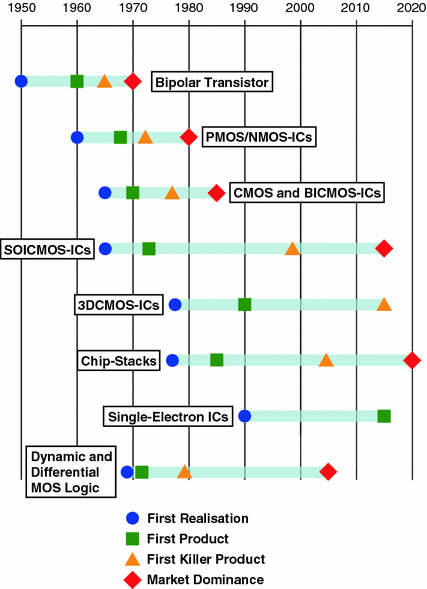
Fig. 1.1
The life-span of chip technologies, 2012 []. Updates: The first 3D-CMOS killer product arrived 2013 with vertical-gate flash memory. Single-electron-transistor first product will not arrive before 2020. Low-voltage, differential logic has arrived, but will dominate only closer towards 2020
1.2 Bipolar-Transistor Technology
Bipolar transistors were identified in [] as the transistor type, which continues to offer the highest drive currents, a favorable transconductance and frequency limits of several hundred GHzat additional manufacturing cost, limited area efficiency and limited compatibility for monolithic, high-density integration with mainstream nano-scale CMOS technologies.
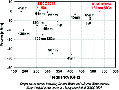
However, their Terahertz capabilities are being pushed further as shown in Fig. ]. The figure shows that Silicon-Germanium offers this performance, outperforming the more expensive Indium-Phosphide transistor technology. Cost-effective heterogeneous 3D integration on large-scale CMOS-chips is the much-needed development for the future of bipolar transistors in nanoelectronics.
Fig. 1.2
Output power versus frequency for THz sources []
1.3 CMOS Integrated Circuits
Circuits on the basis of complementary MOS transistors make up well over 90 % of all ICs. The reduction in transistor size, to achieve higher densities or functionalities, has come to the limits predicted in []. For the key parameter, the length L of the transistor channels:
For Logic: 16 nm,
FOR DRAM: 24 nm
For SRAM: 14 nm
For Flash: 16 nm.
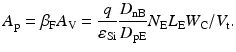
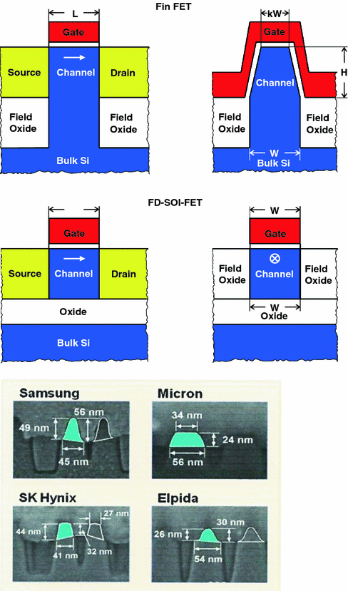
The competition between FinFET and SOI , not considering the cost of manufacturing, can be reduced to the necessary switching energy (CTr + CFan-out + CWire)V2.
The transistor capacitance for the FinFET in Fig. is
where k < 1 accounts for the profile of the fin. In the four cross-section examples, the effective transistor widths (kW + H1 + H2) are about 105, 82, 116 and 56, respectively. This shows that FinFET technologies are drive-current or charge-oriented with large transistor capacitances. The cross-sections shown relate to technologies with about 24 nm minimum features so that the minimum half-pitch of transistor-rows in the direction of current flow would be between 33 and 40 nm.