1.1 From Nanoelectronics to Femtoelectronics
In the year 2000, the first microchips were produced with gate lengths <100 nm, and microelectronics received the new label nanoelectronics. The drive in the industry along the nano-roadmap towards shorter transistors continued in order to build faster processors and to pack more memory bits on each chip. At the same time, the research community had widespread programs running on quantumnanometer-scale phenomena with considerable optimism for near-term practical success. By the year 2010, the planned 32 nm milestone (node) had been reached, including most of the expected chip specifications, but with a twist since 2005: the 3D integration of many thin chips on top of each other, connected through TSVs (through-silicon vias), to enhance the progress on the roadmap. But the year 2010 was also marked by the rapidly growing consensus that the end of the roadmap is near at 15 nm (2016) or 10 nm (2018?) at best, and that none of the new quantum-nano devices will have any economic impact before 20252030 . This poses the serious question: Will the progression of chips come to a standstill, and with it the worlds driving technology (information and communication)? The answer is: Not necessarily, if we accept the nanometer-limit and, at the same time, exchange the nanometer priority for a femtojoule priority: Energy per function , often called the power efficiency , is the new yardstick .
Between 2010 and 2020, the energy per chip function, such as processing, memory, or communication, has to be reduced by a factor of 1,000 if the nanoelectronics market is going to have enough to offer to six billion potential global customers. Remarkably, many of these chip functions run at picojoule (pJ) levels in 2010. The challenge is now to achieve femtojoule (fJ) levels. Therefore we set our focus on moving from nano (meter) to femto (joule) electronics .
The task is challenging indeed, because the nanometer roadmap only offers a final contribution of threefold at best, which may enter as 3=9 in an energy figure-of-merit (FOM), leaving us with another factor of >100 in needed improvements within a decade. One approach to identifying a future strategy is to consider how the remarkable advances in the 100 years of electronics and, particularly, in the past 50 years of integrated circuits were achieved and which repertory of R&D results of the past 30 years could be put to the test in product developments of the present decade. This is the theme of , From Microelectronics to Nanoelectronics.
Our path to the 2020 goals will point out critical electronic functions, which are most challenging and intriguing, since we reach and go below the energy per operation in the synapses of natural brains: The typical energy per operation of a neurons synapse is 10 fJ.
We pose five fundamental questions in this book, and we give answers, all of which point out tough energy requirements on future nanochips so that we conclude: Sustainable nanoelectronics has to be femto(joule) electronics .
Here are the five questions:
Why do we hit the end of the nano-roadmap?
Which femtoelectronic solutions can we find for critical functions?
What are the requirements for new chip products and how can we meet them?
Which radical femtoelectronic solutions should we seek for intelligent computing?
What are the challenges for the femtoelectronics ecosystem of education, research, and business?
How does the 2020 world benefit from femtoelectronic chips?
1.2 Why Do We Hit the End of the Nano-roadmap?
Because microelectronics has advanced so successfully over 50 years with a linear strategy of scaling down transistor sizes, it comes as a surprise that this mode of progression will hit its limits by 2015. We deal with these problems in (nanolithography).
In , we evaluate the future of eight chip technologies, revealing that their development towards a fruitful future took between 25 and more than 35 years, an example being the present emphasis on the 3D integration of chips, which was taken on as a major research topic 30 years ago, only to be put aside in the late 1980s because the 2D scaling strategy did the job well and less disruptively . Transistors with gate lengths of <10 nm on the scaling roadmap were built in the lab and published before 2000. Why are their fundamental problems being considered only now? In Sect. 3.2, we identify two fundamental problems, which are present no matter how precisely we can process these 10 nm transistors:
The atomic variance (only ~5 doping atoms in the channel) makes the spread of transistor thresholds larger than the allowed supply voltage, so not all of them can be turned on or off.
The available voltage gain (because of drain-induced barrier lowering) becomes <1, and without amplification, circuits lose their signals in noise (at least in all electronics operating in natural environments).
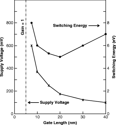
Because of these fundamental limits, we actually find that the most important basic amplifier in modern chip electronics, the CMOS (complementary metaloxidesemicondiuctor) inverter, has its minimum energy per operation at a gate length of 20 nm (Fig. ), because, moving towards 10 nm, we have to raise the supply voltage in order to compensate for the facts listed above. Nevertheless, the switching energy of this fundamental amplifier is just 5 eV=1018 J, which means that we have to move just 25 electrons through a potential difference of 200 mV.
Fig. 1.1
Minimum supply voltage and switching energy of a CMOS inverter as a function of gate length for an equivalent gate-oxide thickness (EOT) of 1 nm
A 10 nm transistor and, for that matter, even a 20 nm transistor, performs this by moving just one electron at a time through the channel at speeds (Fig. ) depending on the instantaneous voltages. That is, practically all minimum transistors with gate lengths <20 nm are single-electron transistors . We present these fundamental details at the outset of this book in order to show that, at the end of the nano-roadmap, we are putting (at least digital) information on single electrons .

