Dragoman Daniela. - 2D Nanoelectronics: Physics and Devices of Atomically Thin Materials
Here you can read online Dragoman Daniela. - 2D Nanoelectronics: Physics and Devices of Atomically Thin Materials full text of the book (entire story) in english for free. Download pdf and epub, get meaning, cover and reviews about this ebook. City: Cham, year: 2017, publisher: Springer International Publishing : Imprint: Springer, genre: Children. Description of the work, (preface) as well as reviews are available. Best literature library LitArk.com created for fans of good reading and offers a wide selection of genres:
Romance novel
Science fiction
Adventure
Detective
Science
History
Home and family
Prose
Art
Politics
Computer
Non-fiction
Religion
Business
Children
Humor
Choose a favorite category and find really read worthwhile books. Enjoy immersion in the world of imagination, feel the emotions of the characters or learn something new for yourself, make an fascinating discovery.

- Book:2D Nanoelectronics: Physics and Devices of Atomically Thin Materials
- Author:
- Publisher:Springer International Publishing : Imprint: Springer
- Genre:
- Year:2017
- City:Cham
- Rating:3 / 5
- Favourites:Add to favourites
- Your mark:
2D Nanoelectronics: Physics and Devices of Atomically Thin Materials: summary, description and annotation
We offer to read an annotation, description, summary or preface (depends on what the author of the book "2D Nanoelectronics: Physics and Devices of Atomically Thin Materials" wrote himself). If you haven't found the necessary information about the book — write in the comments, we will try to find it.
Dragoman Daniela.: author's other books
Who wrote 2D Nanoelectronics: Physics and Devices of Atomically Thin Materials? Find out the surname, the name of the author of the book and a list of all author's works by series.


2D Nanoelectronics: Physics and Devices of Atomically Thin Materials — read online for free the complete book (whole text) full work
Below is the text of the book, divided by pages. System saving the place of the last page read, allows you to conveniently read the book "2D Nanoelectronics: Physics and Devices of Atomically Thin Materials" online for free, without having to search again every time where you left off. Put a bookmark, and you can go to the page where you finished reading at any time.
Font size:
Interval:
Bookmark:

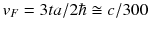 is the Fermi velocity and
 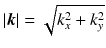 , with
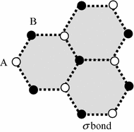
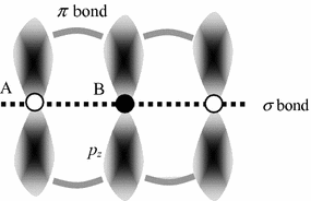
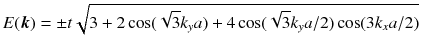
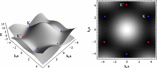
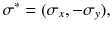
  the wavevector of charge carriers relative to Dirac points. This linear dispersion relation is the hallmark of graphene monolayer and implies that the effective mass of charge carriers vanishes near Dirac points, unlike in common semiconductors. Another difference from common semiconductors is that the transport properties in graphene are the same for electron or hole states, since the dispersion relation is completely symmetric around the Dirac point.
 approximation, the Dirac equation for the graphene monolayer is written as (Wu et al. ):


 with
with 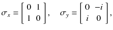
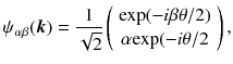
 and
and  represent the spinorial wavefunctions around the K and K points, respectively.
 as
as 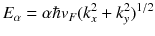

Font size:
Interval:
Bookmark:
Similar books «2D Nanoelectronics: Physics and Devices of Atomically Thin Materials»
Look at similar books to 2D Nanoelectronics: Physics and Devices of Atomically Thin Materials. We have selected literature similar in name and meaning in the hope of providing readers with more options to find new, interesting, not yet read works.
Discussion, reviews of the book 2D Nanoelectronics: Physics and Devices of Atomically Thin Materials and just readers' own opinions. Leave your comments, write what you think about the work, its meaning or the main characters. Specify what exactly you liked and what you didn't like, and why you think so.