Table of Contents
List of tables
- Tables in Chapter 5
- Tables in Chapter 7
- Tables in Chapter 11
List of illustrations
- Figures in Chapter 1
- Figures in Chapter 2
- Figures in Chapter 3
- Figures in Chapter 4
- Figures in Chapter 5
- Figures in Chapter 6
- Figures in Chapter 7
- Figures in Chapter 8
- Figures in Chapter 9
- Figures in Chapter 10
- Figures in Chapter 11
- Figures in Chapter 12
Landmarks
Table of Contents
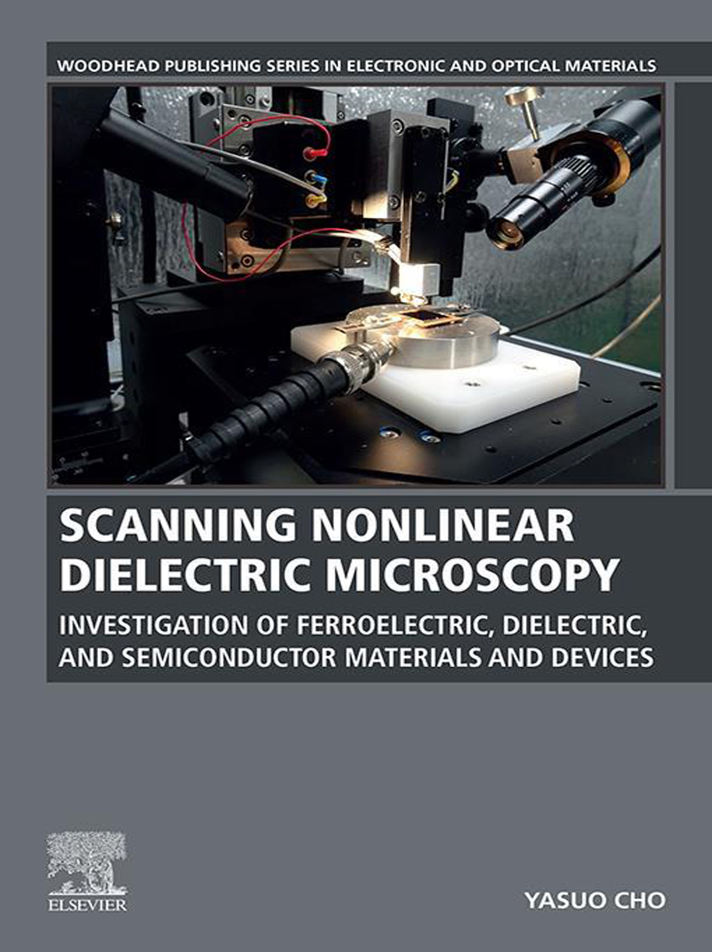
Scanning Nonlinear Dielectric Microscopy
Investigation of Ferroelectric, Dielectric, and Semiconductor Materials and Devices
Yasuo Cho

Copyright
Woodhead Publishing is an imprint of Elsevier
The Officers Mess Business Centre, Royston Road, Duxford, CB22 4QH, United Kingdom
50 Hampshire Street, 5th Floor, Cambridge, MA 02139, United States
The Boulevard, Langford Lane, Kidlington, OX5 1GB, United Kingdom
Copyright 2020 Elsevier Ltd. All rights reserved.
No part of this publication may be reproduced or transmitted in any form or by any means, electronic or mechanical, including photocopying, recording, or any information storage and retrieval system, without permission in writing from the publisher. Details on how to seek permission, further information about the Publishers permissions policies and our arrangements with organizations such as the Copyright Clearance Center and the Copyright Licensing Agency, can be found at our website: www.elsevier.com/permissions.
This book and the individual contributions contained in it are protected under copyright by the Publisher (other than as may be noted herein).
Notices
Knowledge and best practice in this field are constantly changing. As new research and experience broaden our understanding, changes in research methods, professional practices, or medical treatment may become necessary.
Practitioners and researchers must always rely on their own experience and knowledge in evaluating and using any information, methods, compounds, or experiments described herein. In using such information or methods they should be mindful of their own safety and the safety of others, including parties for whom they have a professional responsibility.
To the fullest extent of the law, neither the Publisher nor the authors, contributors, or editors, assume any liability for any injury and/or damage to persons or property as a matter of products liability, negligence or otherwise, or from any use or operation of any methods, products, instructions, or ideas contained in the material herein.
British Library Cataloguing-in-Publication Data
A catalogue record for this book is available from the British Library
Library of Congress Cataloging-in-Publication Data
A catalog record for this book is available from the Library of Congress
ISBN: 978-0-12-817246-9 (print)
ISBN: 978-0-08-102803-2 (online)
For information on all Woodhead Publishing publications visit our website at https://www.elsevier.com/books-and-journals
Publisher: Matthew Deans
Acquisitions Editor: Kayla Dos Santos
Editorial Project Manager: Emma Hayes
Production Project Manager: Anitha Sivaraj
Cover Designer: Matthew Limbert
Typeset by MPS Limited, Chennai, India

Preface
Yasuo Cho, Research Institute of Electrical Communication, Tohoku University
Scanning nonlinear dielectric microscopy (SNDM) was invented in 1994 in Yamaguchi, Japan. Originally it was developed for investigating ferroelectric and dielectric materials with rather small nonlinear dielectric effects through the detection of capacitance variations caused by an applied voltage, that is, dC/dV. Thus since its early days, SNDM has featured a high sensitivity to capacitance variation, on the order of 1022F/Hz  .
.
SNDM can easily measure nanoscale ferroelectric domains under ambient conditions and even atomic-scale dipole moments under ultrahigh vacuum conditions. Moreover, as an application of SNDM to next-generation ultrahigh-density memory devices beyond the magnetic hard disk drive (HDD) and semiconductor flash memory, an investigation of ultrahigh-density ferroelectric data storage based on SNDM has been extensively investigated.
As SNDM has a high sensitivity to capacitance variation, it is also very effective at characterizing semiconductor materials and devices. It can easily distinguish the dopant type (PN) and has a wide dynamic range of sensitivity to both low and high concentrations of dopants. It is also applicable to the analysis of compound semiconductors with much lower signal levels than Si. We can avoid errors due to the two-valued function (contrast reversal) problem of dC/dV signals using dC/dz-SNDM. Extended versions of SNDM have been developed, such as superhigher-order SNDM, local-deep-level transient spectroscopy, noncontact SNDM, and scanning nonlinear dielectric potentiometry. The favorable features of SNDM originate from its significant sensitivity.
Thus this book will meet the needs of those researchers in the industry, as well as academics and students, involved in the fields of ferroelectrics, dielectrics, semiconductors, and scanning probe microscopy.
This book will help those intending to investigate the ferroelectric nanodomain structure, which cannot be resolved by conventional piezoresponse force microscopy (PFM), and the atomic dipole moment, which cannot be distinguished by conventional Kelvin probe force microscopy (KPFM), to realize ultrahigh-density ferroelectric data storage with much higher memory densities compared to flash memories and magnetic HDDs, to visualize the dopant distribution in the fine structure of state-of-the-art mutualized semiconductor devices, to visualize linear permittivities with higher resolution than other capacitance microscopies, to perform operand measurements of the carrier distribution of working semiconductor devices, to visualize the depletion layer distribution of semiconductor devices that cannot be measured by other methods, to visualize the two-dimensional trap (interface state of density, Dit) distribution at the MOS interface, which has never been visualized by other techniques, and to measure real-time (ns range) carrier movement in semiconductor materials and devices.
This book about SNDM gives new insight into the material and device physics of ferroelectrics, dielectrics, and semiconductors, which has proven hard to obtain by other methods.
The author would like to acknowledge the many colleagues and students who have collaborated with and assisted the author in developing many advanced types of SNDM.
Finally, the author wishes to thank his family for their kind encouragement. Without their support and understanding, this book would not be have been published.
September 2019
Chapter 1
Principles of scanning nonlinear dielectric microscopy for measuring ferroelectric and dielectric materials








 .
.