Semiconductor Nanolasers
This unique resource explains the fundamental physics of semiconductor nanolasers and provides detailed insights into their design, fabrication, characterization, and applications.
Topics covered range from the theoretical treatment of the underlying physics of nanoscale phenomena, such as temperature dependent quantum effects and active medium selection, to practical design aspects, including the multi-physics cavity design that extends beyond pure electromagnetic consideration, thermal management and performance optimization, and nanoscale device fabrication and characterization techniques. The authors also discuss technological applications of semiconductor nanolasers in areas such as photonic integrated circuits and sensing.
Providing a comprehensive overview of the field, detailed design and analysis procedures, a thorough investigation of important applications, and insights into future trends, this is essential reading for graduate students, researchers, and professionals in optoelectronics, photonics, applied physics, nanotechnology, and materials science.
Qing Gu is Assistant Professor of Electrical Engineering at the University of Texas at Dallas, where she is directing research in the Nanophotonics Laboratory. Her research interests include the experimental investigation of miniature semiconductor lasers and other nanophotonic devices, novel light-emitting materials, quantum behavior in nanostructures, and integrated photonic circuits.
Yeshaiahu Fainman is Cymer Professor of Advanced Optical Technologies and Distinguished Professor in Electrical and Computer Engineering at the University of California, San Diego. He directs research in the Ultrafast and Nanoscale Optics Group. He is a fellow of the OSA, the IEEE, and SPIE.
Semiconductor Nanolasers
Qing Gu
The University of Texas at Dallas
Yeshaiahu Fainman
University of California, San Diego

University Printing House, Cambridge CB2 8BS, United Kingdom
Cambridge University Press is part of the University of Cambridge.
It furthers the Universitys mission by disseminating knowledge in the pursuit of education, learning, and research at the highest international levels of excellence.
www.cambridge.org
Information on this title: www.cambridge.org/9781107110489
10.1017/9781316275122
Cambridge University Press 2017
This publication is in copyright. Subject to statutory exception and to the provisions of relevant collective licensing agreements, no reproduction of any part may take place without the written permission of Cambridge University Press.
First published 2017
Printed in the United Kingdom by TJ International Ltd. Padstow Cornwall
A catalog record for this publication is available from the British Library.
Library of Congress Cataloging-in-Publication Data
Gu, Qing, 1985 | Fainman, Yeshaiahu.
Semiconductor nanolasers / Qing Gu, The University of Texas at Dallas, Yeshaiahu Fainman,
University of California, San Diego.
Cambridge : Cambridge University Press, 2017. | Includes bibliographical references.
LCCN 2016045371 | ISBN 9781107110489
LCSH: Semiconductor lasers. | Lasers. | Miniature electronic equipment. | Semiconductors. |
Nanostructured materials.
LCC QC689.55.S45 G8 2017 | DDC 621.36/61dc23
LC record available at https://lccn.loc.gov/2016045371
ISBN 978-1-107-11048-9 Hardback
Cambridge University Press has no responsibility for the persistence or accuracy of URLs for external or third-party internet websites referred to in this publication, and does not guarantee that any content on such websites is, or will remain, accurate or appropriate.
Contents
Introduction
The infrastructure that supports modern society, including health care, education, transportation, finance, and scientific and technological research, has become inextricably tied to the continuous progress in the ability to generate, transmit, receive, and process information. While electronic devices integrated in highly complex circuits have enabled this progress, electronic devices and circuits suffer from inherent limitations, namely resistor-capacitor]. Like the first transistors, the first lasers were macroscopic devices, with footprints on the order of centimeters to decimeters.
As the cavity size is reduced with respect to the emission wavelength, interesting physical effects, unique to electromagnetic cavities, arise. Experiments in the radio and microwave frequencies first demonstrated that the spontaneous emission rate of atoms in a cavity could be enhanced or inhibited, relative to their rate of emission in free space. The change in the spontaneous emission rate was found to depend on the geometry of the cavity as well as the orientation and spectra of the atoms [].
1.1 The History of Laser Minimization
To complement micro- and nano-electronics, optical components have undergone a process of miniaturization over the past several decades. Thus, it is not an exaggeration to state that the maintenance and improvement of modern society is directly related to research advancements in photonic devices and circuits. Similar to transistors, the reduction of the size of lasers would enable a higher packing density of devices and lower power consumption].
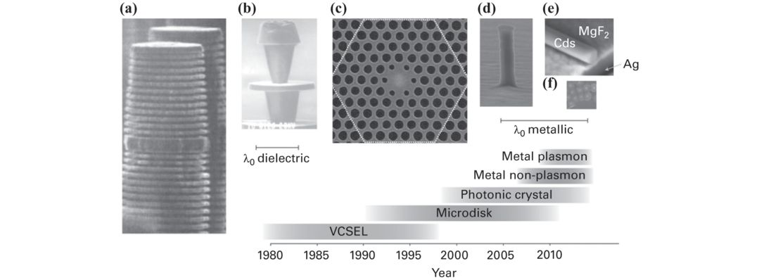
outlines the progress in laser miniaturization over the past few decades. We see from the development time line of small lasers that the evolution of a new laser device usually takes 1020 years: from new laser concept to first proof-of-concept optically pumped demonstration, then to electrically pumped, and in some cases to commercial applications. For practical and commercial insertion of lasers, the devices need to be continuous-wave (CW) current injected at room temperature, ideally with stable emission, reasonably long lifetime and particular properties that the already established types of lasers cannot offer.

Figure 1.1
Development time line of small lasers, from first demonstration to electrical, continuous-wave, and room-temperature operation, and in some cases to commercial applications. Also shown is a size comparison of various types of small lasers. The electron microscopy pictures are scaled to the free-space emission wavelength 0 of each laser: (a) VCSEL, (b) microdisk laser, (c) photonic crystal laser, (d) metallic non-plasmon mode laser; (e) metallic propagating plasmon mode laser; (f) localized plasmon mode laser. The free-space wavelength scale bar of the metal-cavitybased lasers (df) is twice that of the dielectric lasers (ac) to permit details to be seen. The metal-cavity lasers are typically smaller than 0 and dramatically smaller than corresponding dielectric-cavity lasers.
Reprinted from reference [] with permission from Macmillan Publishers Ltd.
. Each type of cavity or laser design has its advantage: for example, photonic crystal dielectric lasers with few-quantum-dot gain show extremely low threshold at cryogenic temperatures; dielectric cavities generally have higher Q factors than metal-clad cavities; and metal-clad cavities have much smaller dimensions than dielectric ones. In the context of subwavelength devices, one of the most figure-of-merit is size.


