 Fundamentals of Ultra-Thin-Body MOSFETs and FinFETs Understand the theory, design, and applications of the two principal candidates for the next mainstream semiconductor-industry device with this concise and clear guide to FD/ UTB transistors. This book * Describes FD/SOI MOSFETs and 3-D FinFETs in detail * Covers short-channel effects, quantum-mechanical effects, and applications of UTB devices to floating-body DRAM and conventional SRAM * Provides design criteria for nanoscale FinFET and nanoscale thin- and thick-BOX planar FD/SOI MOSFET to help reduce technology development time * Projects potential nanoscale UTB CMOS performances * Contains end-of-chapter exercises For professional engineers in the CMOS IC field who need to know about optimal nonclassical device design and integration, this is a must-have resource. Jerry G. Fossum is Distinguished Professor Emeritus of Electrical and Computer Engineering at the University of Florida, Gainesville, and a Fellow of the IEEE. He won the IEEE/EDS J. J.
Ebers Award in 2004 for outstanding contributions to the advancement of SOI CMOS devices and circuits through modeling. Vishal P. Trivedi is a Member of the Technical Staff and a Distinguished Innovator at Freescale Semiconductor, Inc., and a Senior Member of the IEEE. The future of CMOS technology lies in replacing the classical, bulk MOSFET with new transistor structures such as the FinFET and ultra-thin body MOSFET. Those with a solid background in classical MOS device theory will find here an authoritative and comprehensive treatment of the final frontier in CMOS technology. Mark Lundstrom, Don and Carol Scifres Distinguished Professor of Electrical and Computer Engineering, Purdue University Avaluable volume on the design and modeling of silicon-on-insulator and multiple-gate MOSFETs by a pioneer and expert on the subject.
Yuan Taur, University of California at San Diego This is precisely the book everybody in the advanced nano-CMOS world wanted to see out ASAP. Timely, brilliant and most useful - written by a Master (VT) and his own former Master (JF). A life experience is condensed and distilled to provide the necessary ingredients needed for understanding the physics mechanisms and for pursuing with transistor modeling and circuit design. The book is primarily addressed to specialists, engineers and graduate students. This is not a romantic novel about SOI and FinFET affair; it is solid stuff where advanced concepts, strong affirmations and lots of practical equations do not leave space for scientific dust. Sorin Cristoloveanu, CNRS, Grenoble, France This is a timely book about SOI MOSFETs and FinFETs written by one of the leading authorities in the field and his former student.
Since FinFETs have started being imple mented by various companies in production, there is a need for clear understanding of the design trade-offs of such devices. Prof. Fossum, who has done seminal work on model ing SOI MOSFETs since the 1980s, provides a clear elucidation of the physics of these devices. Graduate students, faculty and industrial practitioners should benefit from the pedagogy in this book. Sanjay Banerjee, University of Texas at Austin  Fundamentals of Ultra-Thin-Body MOSFETs and FinFETs JERRY G. FOSSUM University of Florida, Gainesville VISHAL P.
TRIVEDI Freescale Semiconductor, Arizona University Printing House, Cambridge CB2 8BS, United Kingdom Published in the United States of America by Cambridge University Press, New York Cambridge University Press is part of the University of Cambridge. It furthers the Universitys mission by disseminating knowledge in the pursuit of education, learning, and research at the highest international levels of excellence. www.cambridge.org Information on this title: www.cambridge.org/9781107030411 Cambridge University Press 2013 This publication is in copyright. Subject to statutory exception and to the provisions of relevant collective licensing agreements, no reproduction of any part may take place without the written permission of Cambridge University Press. First published 2013 Printing in the United Kingdom by TJ International Ltd. Padstow Cornwall A catalog record for this publication is available from the British Library Library of Congress Cataloging in Publication data Fossum, Jerry G., 1943 Fundamentals of ultra-thin-body MOSFETs and FinFETs / Jerry G.
Fossum, Vishal P. Trivedi. pages cm ISBN 978-1-107-03041-1 (hardback) 1. Metal oxide semiconductor field-effect transistors. 2. I. Title. Title.
TK7871.99.M44F67 2013 621.38150284dc23 2013013370 ISBN 978-1-107-03041-1 Hardback Cambridge University Press has no responsibility for the persistence or accuracy of URLs for external or third-party internet websites referred to in this publication, and does not guarantee that any content on such websites is, or will remain, accurate or appropriate. Contents Preface page Table of physical constants List of symbols List of acronyms Introduction 1.1 Ultimate nanoscale CMOS 1.1.1 Planar FD/SOI MOSFET 1.1.2 FinFET 1.2 Brief overview of the book Unique features of UTB MOSFETs 2.1 Long-channel threshold voltage 2.1.1 The depletion approximation 2.1.2 Review of the classical charge-coupling model 2.1.3 Nonclassical model 2.1.4 Applications 2.1.5 Generalized charge coupling 2.2 Quantum-mechanical effects on Vt 2.3 Short-channel effects on Vt 2.3.1 Modeling 2.3.2 SCE control 2.4 Random-dopant effect on Vt 2.5 Adjustment of Vt 2.5.1 S/D doping-dependent Vt 2.5.2 Sensitivity and RDF analyses 2.6 Currentvoltage characteristics 2.6.1 Classical current formalism with bulk inversion 2.6.2 Quantization and 2-D density of states 2.6.3 Bulk-inversion effects 2.6.4 Carrier mobility 2.7 Gate-source/drain underlap 2.7.1 Effective channel length 2.7.2 Impact of S/D doping profile vi Contents 2.7.3 Insights from optimized 18 nm DG FinFETs 2.7.4 Fringe capacitance 2.8 Charge/capacitance dynamics 2.9 Floating-body effects 2.9.1 Transient BJT effect 2.9.2 FD/UTB floating-body DRAM Exercises Planar fully depleted SOI MOSFETs 3.1 Why thin BOX? 3.1.1 Field fringing in thick BOX 3.1.2 Benefits of BOX-thickness scaling 3.1.3 Challenges with thin BOX 3.2 Basic analyses of scaling and design 3.2.1 2-D effects in the UTB 3.2.2 Vt control via UTB doping? 3.2.3 Vt and SCE control with gate work-function engineering 3.3 Insights on design and scalability with thin BOX 3.3.1 Thin-BOX FD/SOI CMOS design space 3.3.2 LP versus HP design 3.3.3 General insights on GP/bias design for variable Vt Exercises FinFETs 4.1 Triple- or double-gate? 4.1.1 Effects of fin-UTB doping 4.1.2 Effects of bulk inversion 4.1.3 The pragmatic choice 4.2 DG FinFETs 4.2.1 Bulk Si versus SOI 4.2.2 SDG versus ADG 4.2.3 Potential speed superiority 4.2.4 Pragmatic FinFET design 4.3 The ITFET: a hybrid option 4.4 Independent-gate FinFET 4.5 SRAM application 4.5.1 Vt modulation via underlap 4.5.2 Cell design and performance Exercises Appendix UFDG References Index Preface The computer revolution (i.e., faster, smaller, and cheaper computers), and the technol ogies it has enabled (e.g., the Internet, laptops, smart phones), have been driven by continued size-scaling of the CMOS transistors in the constituent integrated circuits (ICs, e.g., the microprocessor) of the computer. This scaling, which has doubled the transistor density on the CMOS IC chip about every two years, has been achieved by simply ratioing the dimensions and related parameters of the basic, classical transistor structure (i.e., the planar single-gate MOSFET in bulk silicon or partially depleted SOI) (Taur and Ning, as improvements in lithography enabled reduced minimum feature size. The CMOS devices have now become so small (e.g., gate lengths are 3040 nm) that this straightforward scaling is no longer possible, mainly because of fundamental limitations in reliable doping of the classical MOSFET. Thus, continued CMOS scaling will require a new, nonclassical transistor structure with ultra-thin body (UTB) that avoids these limitations. The first concrete evidence of the transition to a UTB transistor structure is Intel Corporations adoption of the trigate transistor (or FinFET) (Auth et al., for 22 nm CMOS technology and beyond.
Next page



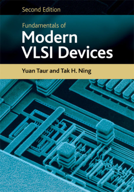
 Fundamentals of Ultra-Thin-Body MOSFETs and FinFETs Understand the theory, design, and applications of the two principal candidates for the next mainstream semiconductor-industry device with this concise and clear guide to FD/ UTB transistors. This book * Describes FD/SOI MOSFETs and 3-D FinFETs in detail * Covers short-channel effects, quantum-mechanical effects, and applications of UTB devices to floating-body DRAM and conventional SRAM * Provides design criteria for nanoscale FinFET and nanoscale thin- and thick-BOX planar FD/SOI MOSFET to help reduce technology development time * Projects potential nanoscale UTB CMOS performances * Contains end-of-chapter exercises For professional engineers in the CMOS IC field who need to know about optimal nonclassical device design and integration, this is a must-have resource. Jerry G. Fossum is Distinguished Professor Emeritus of Electrical and Computer Engineering at the University of Florida, Gainesville, and a Fellow of the IEEE. He won the IEEE/EDS J. J.
 Fundamentals of Ultra-Thin-Body MOSFETs and FinFETs JERRY G. FOSSUM University of Florida, Gainesville VISHAL P.