Chapter 1
Introduction
Jia Di
1Computer Science and Computer Engineering Department, University of Arkansas, Fayetteville, AR, USA
2Department of Electrical Engineering and Computer Science, Texas A&M University-Kingsville, Kingsville, TX, USA
Our world is essentially asynchronous, where time is continuous, and natural influences (e.g., temperature, humidity, illuminance, etc.) can change at any time, not only at predefined increments. Responses of animals and plants are event-driven, not dictated by specific time intervals. When computer scientists and electronic circuit developers create abstractions of our world to design computers and electronic circuits, various approximations are applied. As illustrated in , compared to their analog counterparts, digital design paradigms utilize discrete values to represent their world. Between the two digital paradigms, synchronous logic incorporates a further approximation, representing time as a discrete series of events, by utilizing a periodic clock to signal when change can occur. Asynchronous logic, on the other hand, is a more natural event-driven approach that does not rely on an approximation for time (i.e., there is no synchronizing clock signal).
Table 1.1 Illustration of different computation paradigms
| Discrete time | Continuous time |
|---|
| Discrete value | Digital, synchronous logic | Digital, asynchronous logic |
| Continuous value | Switched-capacitor analog | General analog computation |
This fundamental difference between asynchronous and synchronous logic paradigms grants each with unique design tradeoffs. lists a subset of such tradeoffs. Across all levels of design abstraction (e.g., architectural description, gate-level netlists, transistor-level schematics, and physical layouts), these tradeoffs are translated into various circuit design considerations, such as active/leakage power consumption, propagation delay, throughput, area/size, reliability/robustness, modularity/reusability, noise/emission, design complexity, design automation, etc., which are critical for system architects and circuit designers.
Table 1.2 Subset of tradeoffs between asynchronous and synchronous logic paradigms
| Asynchronous | Synchronous |
|---|
| Continuous time computation | Discrete time computation |
| Local handshaking/self-timed control | Global clock control |
| Observed delay is the average of possible circuit paths, for some paradigms | Observed delay is the maximum overall possible circuit paths |
| Local switching from data-driven computation typically yields lower power operation | Global activity from clock-driven computation requires careful clock gating for low power operation |
| Throughput determined solely by device speed, for some paradigms | Throughput determined by device speed and additional operating margins |
| Data must be encoded for some paradigms, which requires additional wires (e.g., two wires per bit) | Unencoded data acceptable (i.e., one wire per bit) |
1.1 Overview of asynchronous circuits
The theory of asynchronous logic (i.e., circuits being self-timed instead of being externally timed by a periodic clock signal, like synchronous circuits) was first proposed in the 1950s. Since then, many research and development activities on asynchronous circuits have been carried out by both industry and academia, resulting in numerous asynchronous design paradigms being invented and demonstrated in silicon. Asynchronous circuits can be grouped into two broad implementation types, bounded delay (BD) and quasi-delay insensitive (QDI), each with numerous different implementation paradigms. Bounded delay circuits typically utilize a bundled data representation, where data requires one wire per bit (same as synchronous circuits), and includes one additional wire to signal when a group of data wires, referred to as a bundle, is valid. QDI circuits, on the other hand, encode data validity along with the actual data being transmitted, and therefore require more than one wire per bit. An overview of both QDI and BD circuits is provided below.
A typical data encoding for QDI circuits is dual-rail logic, which is a 1-hot encoding requiring two wires per bit, where (D1 = 0, D0 = 1) = DATA0, (D1 = 1, D0 = 0) = DATA1, (D1 = 0, D0 = 0) = absence of DATA, also referred to as the NULL or spacer state, and (D1 = 1, D0 = 1) is an invalid state that will not occur in a properly functioning circuit. Other data encodings are also sometimes utilized, including quad-rail logic (i.e., 1-hot encoding scheme utilizing four wires to represent 2 bits of data) []. These encodings allow the QDI circuit to know when its data are valid without referencing time, and based on this knowledge, to generate handshaking signals to convey this to other parts of the circuit.
Typical QDI circuits alternate between valid DATA states (i.e., all data signals are DATA) and the NULL state (i.e., all data signals are NULL), and utilize a 4-phase handshaking protocol to communicate with neighboring circuits, although some QDI paradigms utilize two-phase handshaking (e.g., [. In Phase 1, the data channel is in the NULL state, and the receiver requests data by asserting the handshaking signal. In Phase 2, data are sent by the sender after receiving the handshaking request by setting the data channel to DATA. In Phase 3, the receiver gets the data and acknowledges this by deasserting the handshaking signal. In Phase 4, the sender resets the data channel back to NULL after receiving the handshaking acknowledgment. After the receiver sees NULL on the data channel, it can request the next data by asserting the handshaking signal, which is Phase 1 again.

Figure 1.1 Four-phase handshaking protocol
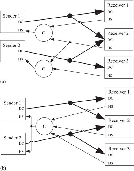
In the general case where a sender transmits to more than 1 receiver, the sender must ensure that all receivers acknowledge the DATA/NULL transmission before sending the subsequent NULL/DATA transmission. This is accomplished by utilizing completion logic consisting of C-elements [ depicts both bit-wise and full-word completion for an example with two senders and three receivers.

Figure 1.2 (a) Bit-wise completion and (b) full-word completion
There are a variety of different QDI paradigms that utilize the typical dual-rail logic and 4-phase handshaking, which vary in terms of combinational logic (C/L) implementation, and partitioning of C/L and registration/latching functionality. Two commonly used QDI paradigms are pre-charge half buffer (PCHB) []. PCHB combines C/L and registration/latching into a single gate structure, which yields a very fine-grained pipeline, while NCL separates C/L and registration/latching functionality, resulting in a coarser-grained pipeline. For feedback loops containing N DATA tokens, at least 2N + 1 asynchronous registers/latches are required to prevent deadlock.

