Bharat Bhushan (ed.) Springer Handbook of Nanotechnology 2nd revised and extended edition 10.1007/978-3-540-29857-1_1 Springer-Verlag 2007
1. Introduction to Nanotechnology
Abstract
A biological system can be exceedingly small. Many of the cells are very tiny, but they are very active; they manufacture various substances; they walk around; they wiggle; and they do all kinds of marvelous thingsall on a very small scale. Also, they store information. Consider the possibility that we too can make a thing very small that does what we wantthat we can manufacture an object that maneuvers at that level.
(From the talk There's Plenty of Room at the Bottom, delivered by Richard P. Feynman at the annual meeting of the American Physical Society at the California Institute of Technology, Pasadena, CA, on December 29, 1959.)
1.1 Nanotechnology Definition and Examples
Nanotechnology literally means any technology done on a nanoscale that has applications in the real world. Nanotechnology encompasses the production and application of physical, chemical, and biological systems at scales ranging from individual atoms or molecules to submicron dimensions, as well as the integration of the resulting nanostructures into larger systems. Nanotechnology is likely to have a profound impact on our economy and society in the early 21st century, comparable to that of semiconductor technology, information technology, or cellular and molecular biology. Science and technology research in nanotechnology promises breakthroughs in areas such as materials and manufacturing, nanoelectronics, medicine and healthcare, energy, biotechnology, information technology, and national security. It is widely felt that nanotechnology will be the next industrial revolution.
Nanometer-scale features are mainly built up from their elemental constituents. Examples include chemical synthesis, the spontaneous self-assembly of molecular clusters (molecular self-assembly) from simple reagents in solution, biological molecules (e.g., DNA) used as building blocks for the production of three-dimensional nanostructures, or quantum dots (nanocrystals) of arbitrary diameter (about 10 to 105atoms). The definition of a nanoparticle is an aggregate of atoms bonded together with a radius between 1 and 100nm. It typically consists of 10 to 105atoms. A variety of vacuum deposition and nonequilibrium plasma chemistry techniques are used to produce layered nanocomposites and nanotubes. Atomically controlled structures are produced using molecular beam epitaxy and organometallic vapor phase epitaxy. Micro- and nanosystem components are fabricated using top-down lithographic and nonlithographic fabrication techniques and range in size from micro- to nanometers. Continued improvements in lithography for use in the production of nanocomponents have resulted in line widths as small as 10nm in experimental prototypes. The nanotechnology field, in addition to fabrication of nanosystems, provides impetus to develop experimental and computational tools.
The discovery of novel materials, processes, and phenomena at the nanoscale and the development of new experimental and theoretical techniques for research provide fresh opportunities for the development of innovative nanosystems and nanostructured materials. The properties of materials at the nanoscale can be very different from those at a larger scale. When the dimension of a material is reduced from a large size, the properties remain the same at first, then small changes occur, until finally, when the size drops below 100nm, dramatic changes in properties can occur. If only one length of a three-dimensional nanostructure is of nanodimension, the structure is referred to as a quantum well; if two sides are of nanometer length, the structure is referred to as a quantum wire. A quantum dot has all three dimensions in the nanorange. The word quantum is associated with these three types of nanostructures because changes in properties arise from the quantum-mechanical nature of physics in the domain of the ultra small. Materials can be nanostructured for new properties and novel performance. This field is opening new venues in science and technology.
Micro- and nanosystems include micro/nanoelectromechanical systems. MEMS refers to microscopic devices that have a characteristic length of less than 1mm but more than 100nm and combine electrical and mechanical components. NEMS refers to nanoscopic devices that have a characteristic length of less than 100nm and combine electrical and mechanical components. In mesoscale devices, if the functional components are on a micro- or nanoscale, they may be referred to as MEMS or NEMS, respectively. These are referred to as intelligent miniaturized systems comprising sensing, processing, and/or actuating functions and combine electrical and mechanical components. The acronym MEMS originated in the USA. The term commonly used in Europe is microsystem technology (MST), and in Japan it is micromachines. Another term generally used is micro/nanodevices. MEMS/NEMS terms are also now used in a broad sense and include electrical, mechanical, fluidic, optical, and/or biological functions. MEMS/NEMS for optical applications are referred to as micro/nanooptoelectromechanical systems (MOEMS/NOEMS). MEMS/NEMS for electronic applications are referred to as radio-frequency-MEMS/NEMS or RF-MEMS/RF-NEMS. MEMS/NEMS for biological applications are referred to as BioMEMS/BioNEMS.
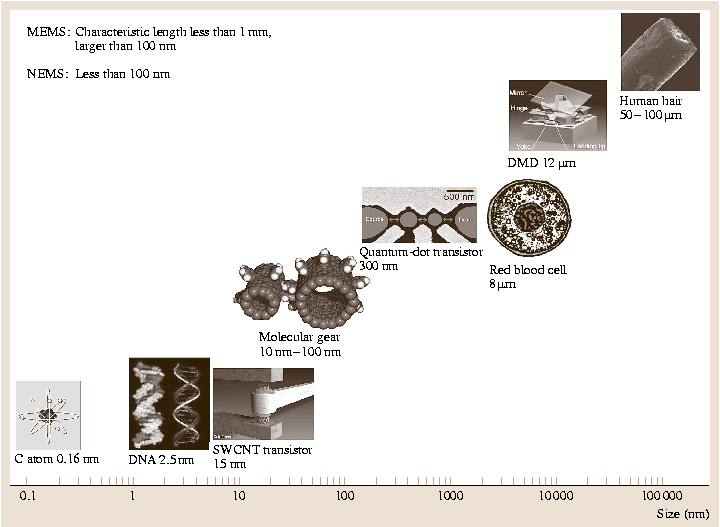
To put the dimensions of MEMS and NEMS in perspective, see Fig.. Individual atoms are typically a fraction of a nanometer in diameter, DNA molecules are about 2.5nm wide, biological cells are in the rage of thousands of nanometers in diameter, and human hair is about 75m in diameter. The NEMS shown in the figure range in size from 15 to 300nm and MEMS is 12000nm. The mass of a micromachined silicon structure can be as low as 1nN, and NEMS can be built with a mass as low as 1020N with cross sections of about 10nm. In comparison, the mass of a drop of water is about 10N, and the mass of an eyelash is about 100nN.
Fig. 1.1
Dimensions of MEMS and NEMS in perspective. MEMS/NEMS examples shown are of a vertical single-walled carbon nanotube (SWCNT) transistor (5nm wide and 15nm high) [], and DMD obtained from www.dlp.com
Table 1.1
Dimensions and masses in perspective.
( a ) Dimensions in perspective |
NEMS characteristic length | < 100nm |