Springer Science+Business Media Singapore 2017
Rajesh Singh and Sushabhan Choudhury (eds.) Proceeding of International Conference on Intelligent Communication, Control and Devices Advances in Intelligent Systems and Computing 10.1007/978-981-10-1708-7_1
Differential Voltage Current Conveyor-Based One-Shot Pulse Generator Circuit Implementation
Amit Bhattacharyya 1
(1)
Department of Electronics and Communication Engineering, Haldia Institute of Technology, Haldia, WB, 721657, India
Abstract
This paper presents a novel One-shot pulse Generator Circuit, which is composed of only one differential voltage current conveyor (DVCC) as the active element. The application circuits utilizing the DVCC are introduced and implemented. Only one DVCC and two resistors and one capacitor are required to construct every circuit. Each circuit is able to provide a pulse-shaped response having changeable width via a positive-edge triggered signal. The first one is a general one-shot pulse generating circuit. The second design can reduce the recovery time after applying triggered signals. Is-Spice is the simulation software to simulate every model. To fabricate the models commercially available ICs (AD844AN) and passive elements are required. Program and experimental outputs satisfy theoretical results.
Keywords
One-shot pulse generator Differential voltage current conveyor Positive-edge trigger Recovery time Parasitic effects
Introduction
One-shot pulse generators are widely used in instrumentation, communication, phase-locked loop circuits, power conversion control circuits, and signal processing applications [] over traditional operational amplifiers, the presented one-shot pulse generator circuit is more applicable than the traditional designs to DVCC-based circuit systems. The proposed model has a number of advantages over the traditional design due to following reasons:
- (1)
Number of active devices used in the model are less or same.
- (2)
Most of the passive components are grounded rather than floating structure to obtain the advantages of IC fabrication techniques and enhanced parasitic properties.
- (3)
Obtained operating frequency is higher than OPA-based structure.
- (4)
The design can shorten the recovery time for triggering signals.
- (5)
Temperature sensitivity is less.
- (6)
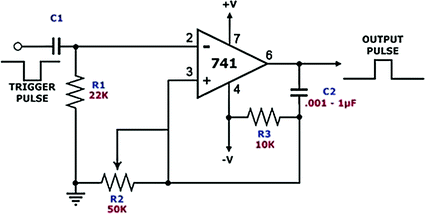
Applicability in fully DVCC-based systems increases (Fig. ).
Fig. 1
Traditional approach of One-shot pulse generator circuit
Circuit Discussions and Working Ideology
2.1 Fundamental Idea and Construction of DVCC
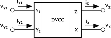
The DVCC is useful for performing various superior presentations of continuous signal processed fields where voltage terminals require high input impedance and current terminals require high output impedance. Circuit symbol of DVCC having four terminals is used here. The voltage drop at X terminal equals the difference of voltage between two Y terminals, and the current flowing through X terminal is same as that of Z terminal. DVCC has zero X terminal input impedance and infinite impedances at two Y and one Z terminals. The circuit symbol of DVCC is shown in the Fig..
Fig. 2
Circuit symbol of DVCC
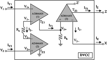
To check the effectivity of projected model, Fig. shows a realistic construction of DVCC using IC844AN which is easily accessible in the market.
Fig. 3
Implementation of DVCC using IC844AN
The difference between AD844AN and OPAs is that it has a virtual short property between the inverting and non-inverting input terminals. Current flow through inverting terminal and current flow through T Z terminal are same. Infinite resistances at two Y terminals are taken from non-inverting input terminals of the first two AD844ANs of DVCC structure. By connecting the T Z terminal of the first IC AD844AN to the non-inverting input terminal of the third through resistor R b which is grounded, voltage drop at X terminal equals the difference of voltage between two Y terminals, and the current flowing through X terminal is same as that of Z terminal, is obtained. From Fig. the following V I characteristic equations can be written as follows:
Therefore, the V I characteristic equations of ideal DVCC can be obtained by setting R a = R b. Figure shows a realistic construction of DVCC using IC844AN which is easily accessible in the market.
2.2 Proposed DVCC-Based Model Discussions
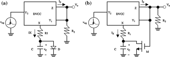
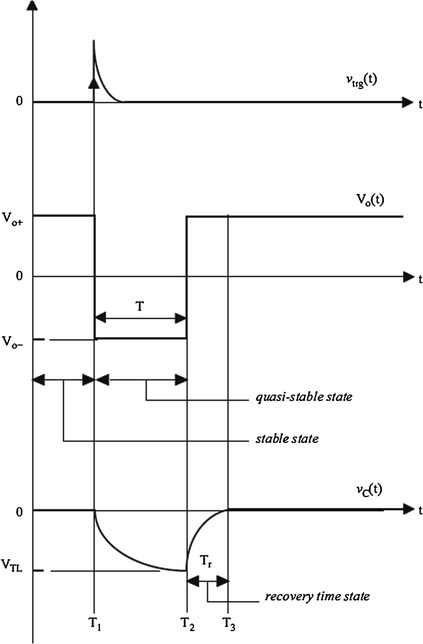
Figure . T represents the pulse width, and Tr is considered as the required time of recovery until later pulse is fired. The working ideology of every proposed model has three conditions: stable condition, quasi stable condition, and recovery time condition. During stable condition, capacitor C is open-circuited and capacitor voltage VC drop is secured by the diode D or the analog switch M . By adjusting R 2 greater than R 1 stable state operation is maintained, for which I Z is less positive than I X . Hence the output voltage V O reaches upper constant level V o+.
Fig. 4
a First projected model and b Second projected model to reduce recovery
Fig. 5
Generated waveforms of the proposed models
This state will continue up to t = T 1, where a trigger pulse is fired and then, the quasi stable condition will start. At present, I z is greater than I x and consequently the output voltage V o jumps abruptly from V o+ to V o. Since V o remains at V o, C starts to discharge through R 1 from t = T 1. In this state, the currents through X and Z terminals, i.e., I x and I z and the capacitor voltage V C ( t ) are expressed as follows:

