Yun-feng Xiao - Ultra-high-q Optical Microcavities
Here you can read online Yun-feng Xiao - Ultra-high-q Optical Microcavities full text of the book (entire story) in english for free. Download pdf and epub, get meaning, cover and reviews about this ebook. year: 2021, publisher: World Scientific Publishing Company, genre: Science. Description of the work, (preface) as well as reviews are available. Best literature library LitArk.com created for fans of good reading and offers a wide selection of genres:
Romance novel
Science fiction
Adventure
Detective
Science
History
Home and family
Prose
Art
Politics
Computer
Non-fiction
Religion
Business
Children
Humor
Choose a favorite category and find really read worthwhile books. Enjoy immersion in the world of imagination, feel the emotions of the characters or learn something new for yourself, make an fascinating discovery.
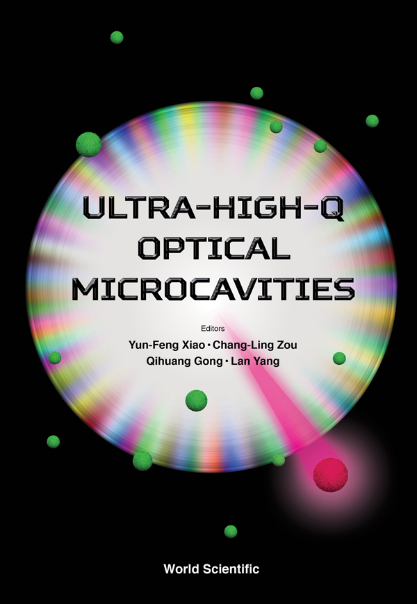
- Book:Ultra-high-q Optical Microcavities
- Author:
- Publisher:World Scientific Publishing Company
- Genre:
- Year:2021
- Rating:4 / 5
- Favourites:Add to favourites
- Your mark:
Ultra-high-q Optical Microcavities: summary, description and annotation
We offer to read an annotation, description, summary or preface (depends on what the author of the book "Ultra-high-q Optical Microcavities" wrote himself). If you haven't found the necessary information about the book — write in the comments, we will try to find it.
Yun-feng Xiao: author's other books
Who wrote Ultra-high-q Optical Microcavities? Find out the surname, the name of the author of the book and a list of all author's works by series.


Ultra-high-q Optical Microcavities — read online for free the complete book (whole text) full work
Below is the text of the book, divided by pages. System saving the place of the last page read, allows you to conveniently read the book "Ultra-high-q Optical Microcavities" online for free, without having to search again every time where you left off. Put a bookmark, and you can go to the page where you finished reading at any time.
Font size:
Interval:
Bookmark:
Cheng Wang
*Department of Electrical Engineering, City University of Hong Kong, Kowloon, Hong Kong, China
HyperLight Corporation, 501 Massachusetts Avenue, Cambridge, MA 02139, USA
John A. Paulson School of Engineering and Applied Sciences, Harvard University, Cambridge, MA 02138, USA
||
Lithium niobate (LN) is an excellent nonlinear optical and electro-optic material that has found many applications in classical nonlinear optics, optical fiber communications and quantum photonics. Here we review the recent development of thin-film LN technology that has allowed the miniaturization of LN photonic devices and microcavities with ultra-high quality factors. We discuss the design principle of LN devices that makes use of the largest nonlinear coefficients, various device fabrication approaches and resulting device performances, and the current and potential applications of LN microcavities.
Since the discovery of optical nonlinearities in the 1960s, lithium niobate (LiNbO3, or LN) has been the most widely used second-order ((2)) material, with applications ranging from nonlinear wavelength conversion for classical and quantum light source,.
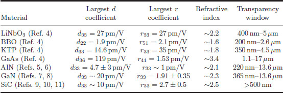
Table 1.1 Optical properties of representative (2) materials (~1,500 nm wavelength).
Since the (2) nonlinear processes are much weaker than linear optical processes, it is a natural choice to use high-Q microcavities to enhance the (2) processes. However, standard photonic device fabrication techniques commonly used in other material systems are not readily compatible with LN, the challenges of which will be discussed in more details in The low index contrast results in weak light confinement and large bending radii (~10 cm), preventing the realization of tightly confined microcavities in LN.
Where there is a will, there is a way, or perhaps more than one way. Many different technological approaches have been extensively studied in recent years in order to realize high-Q microcavities in LN. Along with such technology development, we see a continuous improvement in the Q factors of these cavities, as well as the emergence of a variety of applications.
In this chapter, we provide an overview of basic design principles for LN devices, recent advances in LN fabrication technology, as well as their applications in nonlinear optics and electro-optics.
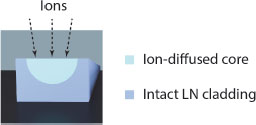
Fig. 1.1 Schematic of traditional ion-diffused waveguides. The low index contrast between the waveguide core and cladding results in large mode areas and weak nonlinear interactions.
Needless to say, most applications of LN photonic devices are closely associated with (2) processes. However, a rigorous mathematic treatment of (2) processes can be quite complicated, since solving a three-wave-mixing process requires tensor analysis at the rank 3. The full (2) tensor has a total of 27 components, connecting the 3 waves and a total of 9 vector field components. Taking sum-frequency generation (1 + 23) as an example, the generated nonlinear polarization at 3 can be expressed as:

where i, j, k {x, y, z}.
Fortunately, in most LN applications, such full treatment is not required. Instead, there is only one critical component out of the 27 the  , since this component is much larger than all other ones. Equation (1.1) can therefore be reduced to a scalar equation. Note that different notations such as d33 and r33 are often used for certain processes, which we will explain next, but keep in mind that they all correspond to .
Long story short, there is only one design rule for almost all LN photonic devices: align the directions of all electric fields with the z axis.
As shown in , taking a z-cut LN crystal as an example, transverse-magnetic (TM) optical modes are preferred for optical waves, and electrical contacts should be placed on top and bottom of the optical waveguide.
For second harmonic generation (SHG) [], where pump light at a frequency of is frequency doubled to a signal frequency of 2, the generated nonlinear polarization at 2 can be expressed as:

where d33 =  is ~30 pm/V for LN and Ez() is the pump electric field z component.
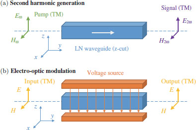
Fig. 1.2 Cross-section illustrations showing the ideal alignment of the electric fields with LN crystal (z-cut in this case) in order to utilize the components. (a) For SHG, TM modes are preferred. (b) For electro-optic modulation, TM optical modes and top-bottom electrodes are preferred.
For electro-optic modulation [], a DC (or microwave) electric field induces a change in optical index of refraction. For LN, the index change for z-polarized light can be expressed as:

where nz is the linear refractive index for z-polarized light, r33 = 30.9 pm/V for LN, and Ez is the DC (or microwave) electric field in z direction.
Just like the majority of silicon photonics integrated circuits rely on silicon-on-insulator (SOI) substrates, a straightforward approach to build nanophotonic devices in LN is to use sub-micron thick, single-crystalline LN films that stand on top of a transparent and lower refractive index substrate, typically silica (SiO2). These substrates are called lithium niobate on insulator (LNOI). The LNOI wafers are fabricated using a Smart-cut ion-slicing process (
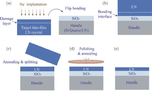
Fig. 1.3 Schematic of LNOI wafer production.
Thanks to the industrial development of LNOI technology in the past decade, high-quality LNOI wafers are now commercially available at sizes up to 4 inches, with various choices of crystal orientations and bottom handles. There are two major choices of LNOI crystal orientations z-cut and x-cut. As we have discussed in
The LNOI production processes also allow for different choices of bottom substrates (). Apart from the possibility of pre-embedding the metal contact layer in the LNOI wafers, popular handle materials include LN, silicon and quartz. LN handles possess the same thermal expansion constants as the device layer, therefore provide the best wafer-bonding quality. Silicon handles offer the possibility of using thermally grown SiO2 as the bottom cladding layer. Thermal SiO2 possesses much lower optical absorption losses than SiO2 grown on top of LN or quartz handles using plasma-enhanced chemical vapor deposition (PECVD). Quartz is an attractive handle material for applications that require high-performance microwave delivery (e.g. high-speed electro-optic modulators) due to its low microwave loss.
Font size:
Interval:
Bookmark:
Similar books «Ultra-high-q Optical Microcavities»
Look at similar books to Ultra-high-q Optical Microcavities. We have selected literature similar in name and meaning in the hope of providing readers with more options to find new, interesting, not yet read works.
Discussion, reviews of the book Ultra-high-q Optical Microcavities and just readers' own opinions. Leave your comments, write what you think about the work, its meaning or the main characters. Specify what exactly you liked and what you didn't like, and why you think so.