Jacques I. Pankove - Optical Processes in Semiconductors
Here you can read online Jacques I. Pankove - Optical Processes in Semiconductors full text of the book (entire story) in english for free. Download pdf and epub, get meaning, cover and reviews about this ebook. year: 2010, publisher: Dover Publications, genre: Computer. Description of the work, (preface) as well as reviews are available. Best literature library LitArk.com created for fans of good reading and offers a wide selection of genres:
Romance novel
Science fiction
Adventure
Detective
Science
History
Home and family
Prose
Art
Politics
Computer
Non-fiction
Religion
Business
Children
Humor
Choose a favorite category and find really read worthwhile books. Enjoy immersion in the world of imagination, feel the emotions of the characters or learn something new for yourself, make an fascinating discovery.
- Book:Optical Processes in Semiconductors
- Author:
- Publisher:Dover Publications
- Genre:
- Year:2010
- Rating:3 / 5
- Favourites:Add to favourites
- Your mark:
Optical Processes in Semiconductors: summary, description and annotation
We offer to read an annotation, description, summary or preface (depends on what the author of the book "Optical Processes in Semiconductors" wrote himself). If you haven't found the necessary information about the book — write in the comments, we will try to find it.
Jacques I. Pankove: author's other books
Who wrote Optical Processes in Semiconductors? Find out the surname, the name of the author of the book and a list of all author's works by series.

Optical Processes in Semiconductors — read online for free the complete book (whole text) full work
Below is the text of the book, divided by pages. System saving the place of the last page read, allows you to conveniently read the book "Optical Processes in Semiconductors" online for free, without having to search again every time where you left off. Put a bookmark, and you can go to the page where you finished reading at any time.
Font size:
Interval:
Bookmark:

I TABLE OF SYMBOLS
II PROPERTIES OF SEMICONDUCTORS
III NOMOGRAPH OF THE TEMPERATURE DEPENDENCE OF THE FERMI LEVEL IN A DEGENERATE PARABOLIC BAND
IV PHYSICAL CONSTANTS
| a | Lattice constant; Bohr orbit |
| c | Velocity of light in vacuum |
| D | Diffusion coefficient |
| E | Energy |
| E c , E v | Energies of conduction- and valence-band edges |
| E g | Gap energy |
| E l | Ionization energy; energy of initial state |
| E A , E D , E x | Binding energies of acceptor, donor, and exciton |
| E F | Fermi level |
| E f | Energy of final state |
| E Fn , E Fp | Quasi-Fermi levels for electrons and for holes |
| E o | Energy needed to create an electron-hole pair |
| E p | Phonon energy |
| E p | Energy of primary electron |
| E T | Threshold for photoelectric emission |
| E t | Energy of trapping level |
| Electric field | |
| F | Force |
| f | Fermi function |
| g | Gain |
| G | Generation rate |
| h | Plancks constant |
| Diracs constant | |
| i, I | Current |
| I o | Saturation current |
| I sc | Short circuit current |
| j, J | Current density |
| k | Boltzmanns constant; wave vector; momentum vector |
| k | Extinction coefficient |
| K | Momentum vector |
| / | Length |
| L | Light intensity |
| L, | Diffusion length for electrons |
| L h | Diffusion length for holes |
| m | Mass of free electron |
| Effective mass of electron | |
| Effective mass of hole | |
| n c | Complex index of refraction |
| n | Real part of index of refraction |
| n | Electron concentration |
| N | Concentration |
| N c , N | Densities of states in conduction and valence bands |
| N A , N a ; N D , N d | Concentrations of acceptors and donors |
| N i | Concentration of impurities |
| N p | Phonon density |
| N T , N t | Concentration of traps |
| P | Probability, pressure, power |
| q | Electron charge |
| Q | Total charge |
| r | Radius |
| R | Reflection coefficient; recombination rate; resistance |
| t | Time |
| T | Temperature, transmission |
| Velocity | |
| V | Voltage, volume |
| V D | Dember voltage |
| V oc | Open circuit voltage |
| Absorption coefficient | |
| Dielectric constant | |
| Work function | |
| B, b | Barrier height |
| Efficiency | |
| K | Specific heat |
| Mobility | |
| v | Frequency |
| Angular frequency | |
| p | Resistivity; density of states |
| Conductivity; capture cross-section | |
| Time constant | |
| Angle | |
| Susceptibility; electron affinity | |
| Energy of the Fermi level with respect to band edge |
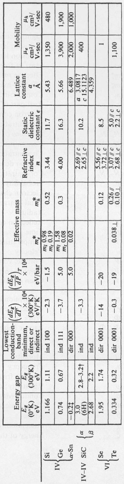
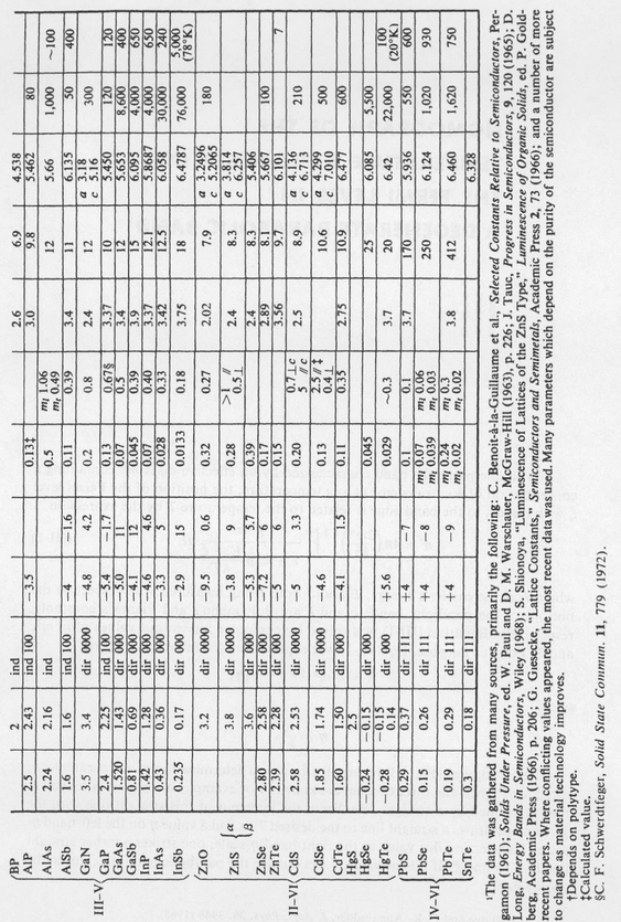
In a simple parabolic band characterized by an effective mass m* containing a concentration of n carriers/cm3 at any temperature, the position of the Fermi level with respect to the band edge is related to the temperature T by the expression
(III-1)
where E is the carriers energy, E and both being measured with respect to the bottom of the parabolic band; k and h are Boltzmanns and Plancks constants, respectively. Equation (III-1) was solved by computer for various values of n, m*, and T. For this purpose, Eq. (III-1) was expressed in the intermediate form
where
The nomograph() permits a graphical determination of any parameter n, m*, , or T when any three of them are known. For example. if n and m* are known, they are joined by a straight line. From the intercept of this straight line with the X - axis one draws a straight line to the desired T tc find a value on the left-hand - scale. Transferring this value to the right-hand - scale, one strikes another straight line to T to find . If is negative, lies outside the parabolic band (i.e., inside the energy gap).
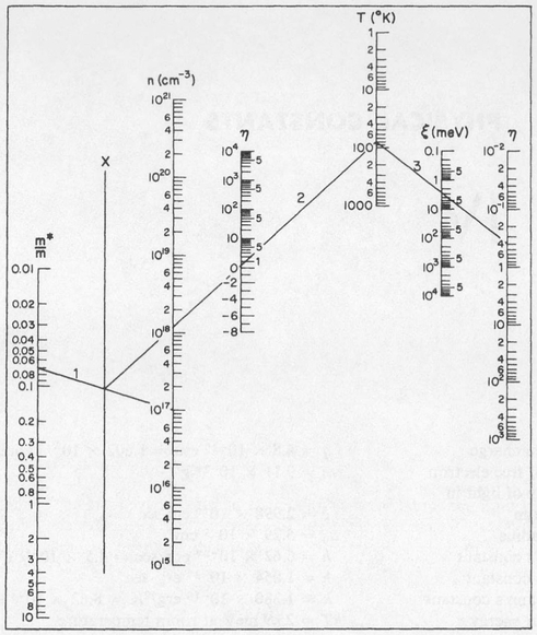
By way of example, the diagram illustrates how one finds the position of the Fermi level at T = 80K in n- type GaAs 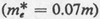 having a carrier concentration n = 1 1017 cm-3. The three steps labeled 1, 2, 3, lead to 3 meV.
Of course, this nomograph is valid only for the case of a temperature-independent free-carrier density and, therefore, it does not apply in the temperature range where carrier freeze-out may occur. Furthermore, a gross approximation is made by assuming that the band is parabolic over the entire range of energies over which the distribution function is appreciable. The neglect of band tailing and of nonpara-bolicity makes the value determined by this nomograph a maximum value.
| Electron charge | q | = 4.8 10-10 esu = 1.602 10-19 coulomb |
| Mass of free electron | m | = 9.11 10-28 g |
| Velocity of light in vacuum | c | = 2.998 1010 cm/sec |
| Bohr radius | a 0 | = 5.29 10-9 cm |
| Plancks constant | h | = 6.62 10-27 erg sec = 4.5 10-15 eVsec |
| Diracs constant | h | = 1.054 10-27 ergs sec |
| Boltzmanns constant | k | = 1.380 10-16 erg/K = 8.62 10-5 eV/ |
| Thermal energy | kT | = 25.9 meV at room temperature |
| = 6.7 meV at liquid-nitrogen temperature |
Font size:
Interval:
Bookmark:
Similar books «Optical Processes in Semiconductors»
Look at similar books to Optical Processes in Semiconductors. We have selected literature similar in name and meaning in the hope of providing readers with more options to find new, interesting, not yet read works.
Discussion, reviews of the book Optical Processes in Semiconductors and just readers' own opinions. Leave your comments, write what you think about the work, its meaning or the main characters. Specify what exactly you liked and what you didn't like, and why you think so.