Filip Tuomisto - Characterisation and Control of Defects in Semiconductors
Here you can read online Filip Tuomisto - Characterisation and Control of Defects in Semiconductors full text of the book (entire story) in english for free. Download pdf and epub, get meaning, cover and reviews about this ebook. year: 2019, publisher: The Institution of Engineering and Technology, genre: Home and family. Description of the work, (preface) as well as reviews are available. Best literature library LitArk.com created for fans of good reading and offers a wide selection of genres:
Romance novel
Science fiction
Adventure
Detective
Science
History
Home and family
Prose
Art
Politics
Computer
Non-fiction
Religion
Business
Children
Humor
Choose a favorite category and find really read worthwhile books. Enjoy immersion in the world of imagination, feel the emotions of the characters or learn something new for yourself, make an fascinating discovery.
- Book:Characterisation and Control of Defects in Semiconductors
- Author:
- Publisher:The Institution of Engineering and Technology
- Genre:
- Year:2019
- Rating:3 / 5
- Favourites:Add to favourites
- Your mark:
Characterisation and Control of Defects in Semiconductors: summary, description and annotation
We offer to read an annotation, description, summary or preface (depends on what the author of the book "Characterisation and Control of Defects in Semiconductors" wrote himself). If you haven't found the necessary information about the book — write in the comments, we will try to find it.
Understanding the formation and introduction mechanisms of defects in semiconductors is essential to understanding their properties. Although many defect-related problems have been identified and solved over the past 60 years of semiconductor research, the quest for faster, cheaper, lower power, and new kinds of electronics generates an ongoing need for new materials and properties, and so creates new defect-related challenges.
This book provides an up-to-date review of the experimental and theoretical methods used for studying defects in semiconductors, focussing on the most recent developments in the methods. These developments largely stem from the requirements of new materials such as nitrides, the plethora of oxide semiconductors, and 2-D semiconductors - whose physical characteristics and manufacturing challenges are much more complex than in conventional Si/Ge or GaAs. Each chapter addresses both the identification and quantification of the defects and their characteristics, and goes on to suggest routes for controlling the defects and hence the semiconductor properties. The book provides valuable information and solutions for scientists and engineers working with semiconductors and their applications in electronics.
Filip Tuomisto: author's other books
Who wrote Characterisation and Control of Defects in Semiconductors? Find out the surname, the name of the author of the book and a list of all author's works by series.


Characterisation and Control of Defects in Semiconductors — read online for free the complete book (whole text) full work
Below is the text of the book, divided by pages. System saving the place of the last page read, allows you to conveniently read the book "Characterisation and Control of Defects in Semiconductors" online for free, without having to search again every time where you left off. Put a bookmark, and you can go to the page where you finished reading at any time.
Font size:
Interval:
Bookmark:
Characterizing electrically active defects by transient capacitance spectroscopy
Lasse Vines
1Department of Physics, University of Oslo, Oslo, Norway
Defects define to a large extent the functionalities of a semiconductorthey are the catalyst for electrical conduction and optical interaction but can at the same time be detrimental to device performance. These defects, or perturbations to a semiconductor lattice, can be of intrinsic nature, for example, a vacancy or self-interstitial, or extrinsic, such as an impurity atom. Some of these defects are electrically inactive and will not be considered in this chapter. The properties of electrically active defects have been intensely studied for decades, but the topic remains a crucial part of semiconductor science. Electrically active defects form states in the forbidden band gap, and these states can donate or accept electrons to or from the conduction band (the lowest range of available electron states) or the valence band (the highest range of electron energies in which electrons are normally present ). Electronic states formed close to the bottom of the conduction band or top of the valence band are labeled shallow, typically formed by substitutional impurities and used as dopants. Deep defects are found further away from the band edges and are present in all semiconductors. Examples of such defects are impurity atoms, intrinsic defects (e.g., vacancies, interstitials, and antisite defects), or complexes between them. The present chapter will discuss properties and techniques to electrically characterize deep-level defects in semiconductors. In particular, spectroscopic characterization techniques based on measuring capacitance transients will be a main focus, with deep-level transient spectroscopy (DLTS) as a prime example.
In traditional and well-developed semiconductors such as silicon (Si) and gallium arsenide (GaAs), many of the deep levels have been identified and thoroughly studied. This identification and characterization of the deep levels by DLTS and related techniques have given us a unique insight into point defects and their behavior, but even deep-level defects in Si remain an active field of research where important defect-related topics remain unresolved. Further, as new semiconducting materials are being explored, a crucial part of understanding their properties is the formation of electrically active deep defectssince these may ultimately determine the electrical performance of the material.
In early studies of deep-level defects, techniques such as Glow curve [].
In this chapter, characterization of electrically active defects is discussed and transient capacitance measurement techniques are addressed. The chapter starts by introducing the main properties describing the electrical activity of a defect, before techniques to measure these properties using thermal and optical emission are discussed. Key techniques based on measuring capacitance transients are reviewed, with particular emphasis on DLTS, including how DLTS can be utilized for direct measurements of capture cross sections and defect profiles. The latter part of the chapter shows examples of use, where defect studies in silicon is chosen as a well-established material where most of the defect levels are identified, but where fundamental knowledge of the defects can still be gained. Defects in zinc oxide (ZnO) is also discussed and chosen as a less studied material where direct identification of the origin of the defect levels remains an important challenge.
To fully understand the influence of a defect on the electrical properties of a material or a device, a range of parameters needs to be obtained. Consider a point defect having a state in the band gap with an energy Et below the conduction band edge (Ec). According to Shockley, Read [ will be dominating. If the dominating process is trapping of electrons from the conduction band with the subsequent reemission to the conduction band, the center acts as a trap, and if the trapping of the electron is followed by a trapping of a hole from the valence band, i.e., a recombination of an electron hole pair, the level acts as a recombination center, whereas in a generation process, trapping of an electron from the valence band is followed by emission of the electron to the conduction band. The dominating process depends on the position of the level in the band gap and the capture cross sections for electrons and holes. Defect levels located in the upper half of the band gap often have larger rates for the electron emission (en) compared to that of the hole emission (ep) because (EcEt) < (EtEv), where Ev is the valence band edge. Therefore, they mostly interact with the conduction band and capture and emit electrons. It is then labeled an electron trap and often with E as a prefix. The converse holds for hole traps. It is also useful to distinguish between majority and minority carriers, relating electron and hole traps to the prevailing conductivity in the material. In n-type materials, electron traps act as majority carrier traps, and hole traps are labeled minority carrier traps, while the opposite holds for p-type material.
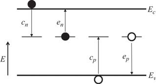
Figure 1.1 Schematics of the charge carrier processes to and from a defect level, showing the capture (cn) and emission (en) of electrons from the conduction band (Ec), and capture (cp) and emission (ep) of holes from the valence band (Ev)
Deep levels are also described as having donor or acceptor character according to their charge state before or after capturing an appropriate carrier. The convention used is found in , where a donor is neutral when filled with an electron, while an acceptor is negative.
Table 1.1 Charge states of donors and acceptors when occupied or not occupied by an electron
| Full | Empty | |
|---|---|---|
| Donor | Neutral | Positive |
| Acceptor | Negative | Neutral |
Thus, important electrical parameters include the energy position and concentration of the defect level, the thermal and optical capture rates for electrons and holes, and the thermal and optical emission rates for electrons and holes.
Trapping of electrons from the conduction band and holes from the valence band occur at rates of cn and cp, respectively. The capture rates can be defined as

where n and p are the concentrations of electrons in the conduction band and holes in the valence band, respectively, n,p is the capture cross section of an electron or a hole, 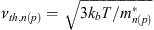 is the electron (hole) thermal velocity, kb is the Boltzmann constant, T is the temperature, and m* is the effective mass of electrons or holes. The capture cross sections are dependent on the charge state of the defect center; a Coulomb attractive defect center normally has a significantly larger cross section than an initially neutral center which, in turn, has a larger cross section than a Coulomb-repulsive center. As a rule of thumb, an attractive, neutral, and repulsive center has corresponding capture cross sections on the order of 1014 or higher, 10151017 and 1019 cm2 or lower. If there are
Font size:
Interval:
Bookmark:
Similar books «Characterisation and Control of Defects in Semiconductors»
Look at similar books to Characterisation and Control of Defects in Semiconductors. We have selected literature similar in name and meaning in the hope of providing readers with more options to find new, interesting, not yet read works.
Discussion, reviews of the book Characterisation and Control of Defects in Semiconductors and just readers' own opinions. Leave your comments, write what you think about the work, its meaning or the main characters. Specify what exactly you liked and what you didn't like, and why you think so.