Springer Nature Singapore Pte Ltd. 2017
Saurabh Nagar and Subhananda Chakrabarti Optimisation of ZnO Thin Films 10.1007/978-981-10-0809-2_1
1. Introduction
Abstract
Extensive research is currently carried out on ZnO as a potential material for the fabrication of optoelectronic devices such as photodiodes, laser diodes (LDs) and light-emitting diodes (LEDs) in the ultraviolet region because of its wide bandgap (3.437 eV at 2 K) and a large excitonic binding energy of 60 meV at room temperature. However, because of intrinsic defects such as oxygen vacancies and zinc interstitials, ZnO is intrinsically deposited as an n-type material. Being a IIVI semiconductor compound, group I and group V elements are considered suitable p-type dopants for ZnO. In this monograph, authors concentrate mostly on the different methods undertaken to achieve strong, reliable and stable p-type ZnO films. Ion implantation, being a suitable technique to achieve selective and localised doping, was used to dope ZnO with different group I and group V elements. Lithium and phosphorus ions were implanted using the conventional ion implantation technique, while plasma immersion ion implantation was used to implant phosphorus and nitrogen ions in the ZnO thin films. Such studies would bring interesting revelations in the optoelectronics field for the ultraviolet range and help to produce devices for the commercial market at a much cheaper cost.
In recent years, researchers across the globe have shown great interest in zinc oxide (ZnO) as a semiconductor material, primarily due to its interesting prospects in the field of optoelectronics applications owing to its wide and direct bandgap (~3.437 eV at 8 K) [1]. In fact, ZnO has become a strong competitor of gallium nitride (GaN), another wide bandgap semiconductor (~3.4 eV at 300 K), as they share most common properties. However, due to its large exciton-binding energy of 60 meV (GaN: 2125 meV), the devices fabricated from ZnO have a much greater probability of surviving at higher temperature. Moreover, ZnO is highly resistant to radiation damage required for space applications. Finally, in terms of suitability for wet etching, the availability of high-quality ZnO bulk crystals and the potentially lower cost for ZnO-based devices, ZnO ranks higher than GaN as well as other transparent conductors like indium tin oxide (ITO). Therefore, ZnO is capable of replacing its competitors in the near future [2, 3].
ZnO growth is possible with most known processes, including chemical vapour deposition (CVD), molecular beam epitaxy (MBE), RF sputtering and pulsed laser deposition (PLD), among others. Due to its large exciton-binding energy, it can also be used for near-band edge emission (NBE) at room temperature and higher temperatures. ZnO has also been a suitable candidate for space applications due to its high resistance to radiation damage. Recently, ZnO has also found applications in transparent thin film transistors [1].
1.1 Material Properties
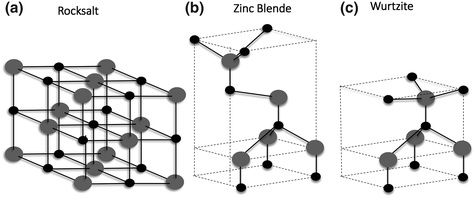
Most of the IIVI binary compound semiconductors crystallise as either zinc blende or hexagonal wurtzite structure where each anion is surrounded by four cations or vice versa. The crystal structure of ZnO is wurtzite (B4), zinc blende (B3) and rock salt (B1), as shown in Fig.. Of these, wurtzite structure is the thermodynamically stable phase in ambient conditions. The zinc blende structure is stabilised only by growth on cubic structures, while rock salt structure can be obtained at high pressures [1].
Fig. 1.1
Representation of ZnO crystal structures: a rocksalt, b cubic zinc blende and c wurtzite. The gray and black spheres denote Zn and O atoms respectively
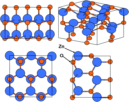
The wurtzite structure has a hexagonal unit cell with lattice parameters, a and c. Figure shows the wurtzite structure of ZnO [4]. The structure is composed of two hexagonal-close-packed sub-lattices, each of which consists of one type of atom displaced with respect to each along the c-axis [1].
Fig. 1.2
Crystalline forms of ZnO in the wurtzite structure
As mentioned earlier, ZnO has many important properties that make it a deserving candidate for primacy in the semiconductor industry. Some of its properties are wide bandgap, large exciton-binding energy and high resistance to radiation damage, among others. ZnO has a melting point of 1975 C and is insoluble in water and alcohol, but can be dissolved in dilute acids. Some of the other properties of ZnO are given in Table [5].
Table 1.1
Properties of ZnO
Properties | Specifications | Comments |
|---|
Structure | Wurtzite | Same as hexagonal |
Bandgap | 3.3 eV | Wide bandgap semiconductor |
Exciton-binding energy | 60 meV | Higher than GaN (2125 meV) |
Piezoelectricity | 1.2 cm2 | Highest among all semiconductors |
Hardness | ~5 | For single crystal |
Toxicity | Very low | Same as other compound semiconductors |
1.2 Electronics Properties
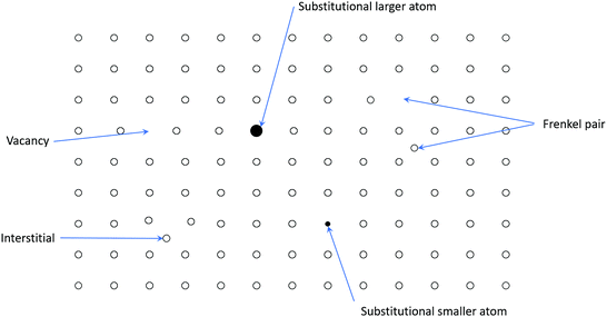
ZnO is intrinsically an n-type semiconductor material due to the existence of native defects such as zinc interstitials (Zn i ) and oxygen vacancies (VO), as well as the presence of impurities in the form of hydrogen, which act as donor states in ZnO [6, 7]. A vacancy is an unoccupied lattice site, which results in an unsatisfied bond within lattice. A vacancy is created when species leave lattice sites and move to the surface. Interstitial defects are present if species do not occupy the lattice site but remain in crystal and disturb the ideal structure of the crystal. Figure shows the various defects present in a crystal [8]. The bulk electron mobility is in the range of 200400 cm2/Vs, which is limited by the acoustic and phonon scattering. However, in the case of thin films, the electron mobility is typically in the range of 1100 cm2/Vs due to the interface roughness and grain boundary scattering [3]. A major obstacle in fabricating ZnO-based bipolar devices is the difficulty of achieving high-quality, reliable and reproducible p-type ZnO. Thus, there are not much data on the hole transport in p-type ZnO due to the problems associated with obtaining p-type ZnO. This lack of data explains why the commercial usage of ZnO-based bipolar devices has not yet been realised in the research community, although it has so many advantages over other materials.
